Koreas Halvha Semitech Bets on Packaging as Chp Value Chain Shifts
Hanwha Semi is showing off FOPLP and hybrid bonding equipment at Semicon Taiwan, signaling South Korea's push into the next layer of the semiconductor value chain as AI chips demand more advanced packaging.
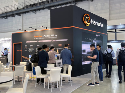
The Packaging Play Nobody Outside Asia Is Watching
Western semiconductor coverage fixates on fabs, design, and the Ukraine war’s impact on gas supplies. But at Semicon Taiwan this week, Hanwha Semitech is quietly making a case that the next battleground for AI chips isn’t lithography — it’s packaging.
The company is unveiling four pieces of equipment, including what it calls the SFM5 Square, its first fan-out panel-level packaging (FOPLP) tool. It’s a move that positions a Korean firm directly against TSMC and Intel, the two giants currently leading the charge on advanced packaging for next-generation processors.
This is the kind of story that gets buried under earnings reports and supply chain panic. It matters because the value chain is shifting, and Korea wants a bigger slice of the pie.
Why Packaging Is the New Frontier
AI chips are getting denser. GPUs need more memory bandwidth. And that means cramming more dies together in a smaller footprint. The traditional approach of building larger single chips hits physical and economic limits — so the industry is turning to advanced packaging as the path forward.
Fan-out panel-level packaging is particularly interesting. Instead of working on circular silicon wafers, which lose a lot of real estate at the edges, FOPLP uses 600-by-600-millimeter square panels. You get more chips per pass, less wasted material, and lower cost per unit. For an industry that can’t afford to waste anything, that math is compelling.
TSMC has been pushing its InFO and CoWoS technologies for years. Intel is betting big on its Foveros and EMIB platforms. Hanwha Semitech is arriving with a full portfolio covering the spectrum from 2.5D to 3D to hybrid bonding — all in one showing.
What Hanwha Is Actually Showing Off
The SFM5 Square is the headline act, but the other three tools tell a bigger story about the company’s ambition.
The SFM5 Expert is a 3D thermocompression bonder for HBM stacks — the high-bandwidth memory that every AI chip maker now needs. Hanwha says it started mass production last year and has been collecting orders since. That’s significant because HBM stacking is one of the most technically demanding processes in modern chipmaking.
The SFM5 TnR is a chip-on-wafer bonder that can join wafer-form logic chips with individual HBM dies in a single tool. That’s a simplification of what has traditionally been a multi-step process, and simplicity in packaging is like gold — it means faster throughput and fewer failure points.
Then there’s the SHB2 Nano, a hybrid bonder the company developed in February this year. It bonds copper electrodes directly to insulators, eliminating the bumps that traditional approaches require. Less distance between chips means faster data transfer and higher integration density. For next-generation HBM, this is the equipment that could define the difference between a good stack and a great one.
Who Wins, Who Loses
If Hanwha Semitech executes on this portfolio, several things shift.
Equipment suppliers in Japan and the US — Tokyo Electron, ASML, KLA — dominate the front end of chipmaking. But packaging equipment has been a smaller, less contested market. A Korean firm arriving with a full suite across multiple packaging technologies would disrupt the assumptions that have held for decades.
TSMC and Intel benefit from having packaging integrated into their foundry models. If an equipment maker can ship tools that rival those capabilities, the economics of vertical integration start to look different. That’s good news for fabless designers who want packaging flexibility without locking into a single foundry.
On the other side, companies that relied on packaging being a simpler, commoditized step in the process are now facing a reality where the equipment itself becomes a competitive differentiator. That’s a harder market to navigate.
The Export-Control Angle
There’s another reason this story deserves more attention outside East Asia. US export controls have complicated China’s access to advanced semiconductor equipment, pushing Chinese firms to develop domestic alternatives. But those controls also create gaps — especially in packaging, where the regulatory focus has been thinner.
Korean equipment makers are positioned to fill some of those gaps. The question isn’t whether they’ll try; it’s how far they can go before geopolitical pressure changes the calculus. Hanwha Semitech’s push into FOPLP and hybrid bonding comes at a time when the US is increasingly scrutinizing what Chinese companies can buy and build.
The company’s own statements about expanding cooperation with global semiconductor manufacturers suggest it’s already thinking about the geopolitical landscape. Partnerships in Taiwan, collaborations with Chinese firms, supply chain diversification — these are all variables that will shape how far this portfolio can go.
What Happens Next
Semicon Taiwan is a trade show, not a product launch. The real test will be whether customer orders follow. Hanwha Semitech has already secured orders for the SFM5 Expert, which is a signal that at least one segment of the market is listening.
But FOPLP is still early days. The technology needs to prove itself at volume before it can claim any share of the advanced packaging market. And the competition from TSMC and Intel isn’t going to wait.
What’s clear is that the conversation about where the semiconductor industry is heading is incomplete without talking about packaging. The hardware wars get the headlines, but the equipment underneath them — the bonders, the aligners, the panel handlers — is what actually makes the whole thing possible. Hanwha Semitech is betting that the next wave of value in semiconductors flows through those tools.
The question is whether the world is ready to pay attention.