Korea Just Solved the Graphene Problem the World Couldnt
A Korean research team used a mundane industrial technique to coat multi-layer graphene on conductors at room temperature — a shift that could slash global power losses and redraw the materials supply chain away from Japanese and European incumbents.
The quiet breakthrough no one outside Korea is talking about yet
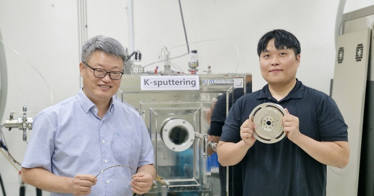
A team at the Korea Electric Power Research Institute (KERI) has done something the materials-science world has chased for over a decade and failed to deliver at scale: coating multi-layer graphene onto conductive substrates at room temperature using an industrial thin-film process that exists on factory floors right now.
The finding, published in Surface & Coatings Technology — a Q1 journal in the surface and coating field — may sound incremental until you consider what it unblocks. Graphene has long been hyped as the ideal conductor when combined with copper. Higher thermal stability, lower electrical resistance, less heat generation. But the problem was always the process. High-quality graphene requires either chemical vapor deposition at extreme temperatures or elaborate transfer techniques that leave behind defects, residue, or both. Those methods are non-trivial to scale. They are expensive to maintain. And they have kept graphene conductors firmly in the lab for more than twenty years.
KERI researchers — led by Dr. Kim Ho-seop at the institute’s Power Cable Research Center, working with teams at Incheon National University and Kyungpook National University — found the root cause of the structural interference that had been blocking clean graphene formation, then simply flipped the approach. Instead of trying to grow pristine graphene and then transfer it, they used conventional sputtering to deposit carbon as a thin film directly onto a substrate at room temperature. The result is a layered structure that builds like Lego blocks: single and double graphene layers, transitioning into graphite stacks, all formed in a single operation without the need for post-processing transfers.
According to KERI, no one has produced a well-ordered carbon thin film this way before. The institute holds four patent filings — three domestic, one international — on the technique.
Why this matters right now
The timing is not accidental. Two forces are compressing the timeline between lab breakthrough and factory floor: the explosion of electric vehicles and the relentless expansion of AI data centers. Both are demanding more power through the same physical wires. A copper conductor of a given gauge has a fixed ceiling. Push more current through it and it heats up. Heat means resistance rises. Resistance means energy is lost as waste. That waste is measured in gigawatt-hours at the scale of national grids.
A composite conductor — copper core wrapped or layered with graphene — would lower resistance, carry more current at the same temperature, and shed less energy over distance. The difference sounds small on a single cable. Over thousands of kilometers of transmission lines, it is enormous. The International Energy Agency has estimated that global electricity transmission and distribution losses hover around 8 to 10 percent of total generated power. Even a fractional improvement compounds to billions of dollars in avoided waste annually.
But the broader implication is supply chain. For years, the materials world has treated graphene as a foreign solution — largely sourced from or controlled by Japanese and European players who invested early in CVD equipment and transfer protocols. Korea has not been absent from graphene research, but it has not dominated the narrative. This shift changes that. The sputtering process KERI used is not exotic. It is the kind of deposition technology installed in dozens of factories across East Asia for semiconductor and display manufacturing. The gap between what Korea proved in a lab and what a cable manufacturer can run tomorrow is far narrower than it was before.
Who wins, who loses
The immediate winner is Korean cable infrastructure. If KERI’s partners or their industry collaborators can translate this into pilot runs within the next two to three years — a reasonable assumption given the maturity of the underlying sputtering equipment — South Korea will hold the only scalable pathway to room-temperature multi-layer graphene conductors. That gives Korean utilities and manufacturers a window of advantage, however brief.
Japanese incumbents in advanced conductor materials face compression. Companies like Furukawa Electric and Sumitomo Electric have invested heavily in high-temperature graphene synthesis and specialized cable solutions. Their moat was process complexity. Korea just made that moat a liability — their existing R&D tracks become dead ends if sputtering at room temperature becomes the standard. European firms in the same space face the same pressure.
The losing side is less obvious but worth naming: the global grid. Right now, most new transmission projects are built with conventional copper or aluminum conductors because the alternatives are too costly or unproven at scale. If graphene-coated conductors reach commercial viability within the next five years, existing infrastructure contracts and procurement pipelines will need to adjust. Utilities that locked in long-term supply agreements for traditional conductors may find themselves on the wrong side of a cost curve shift.
What comes next
The paper is real. The patents are filed. But patents are not products. The next milestone is a pilot-scale run — coating a meaningful length of conductor and measuring whether the lab results hold under industrial conditions. KERI and its university partners have not yet announced a commercialization timeline or a partner manufacturer, which is unusual for an institute of this size and suggests the team is still working through proprietary details before committing publicly.
There is also the question of cost. Graphene at laboratory scale is one thing. Graphene at the tonnage required for national grid upgrades is another. Sputtering is slower than drawing a wire. Even if the process is room-temperature, throughput matters. Any utility evaluating these conductors will want to see cycle-time data, not just resistance numbers.
What is clear is that the barrier to entry has dropped. The hardest part — making graphene stick to a conductor without destroying its structure — is solved. The rest is engineering. For a country that has spent the last decade positioning itself as a materials-science player rather than just a consumer of foreign technology, this breakthrough is a signal. Korea is no longer waiting for someone else to industrialize graphene. It is building the factory floor underneath it.