Samsung's PIM Pivot Proves Moore's Law Is Already Broken
Samsung's first public compute-in-memory benchmarks on an 8B-parameter AI model — 2.3x faster, 3x the throughput — signal a quiet admission: the AI chip arms race can't be won by squeezing more transistors out of HBM alone. The real bottleneck has always been the wire.
The number that changes everything
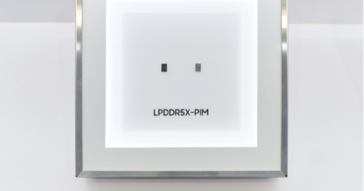
At Hot Chips 2026 on Stanford’s campus, Samsung’s Hwang Garom stood in front of a semiconductor community that had spent the previous four years watching HBM prices surge while bandwidth gains flattened. He then placed one slide on the screen that quietly undermined the entire narrative: Llama 3.1 running on Samsung’s own LPDDR5X-PIM completed an 8-billion-parameter inference pass in 5.4 seconds. The same model on a standard LPDDR5X module took 12.3 seconds.
The throughput jumped from 27 tokens per second to 81.3. A threefold increase — in a memory controller, not a GPU.
This matters because the industry’s mental model for AI acceleration has been brittle for some time. Everyone assumed the answer was more HBM, wider buses, better stacking. The assumption was that if you could just move data fast enough from memory to compute, the problem was solved. Samsung’s public benchmarks demonstrate that assumption is wrong for a growing class of workloads.
Moore’s law didn’t die. It just stopped helping the right problem.
The semiconductor industry’s framing of the AI hardware crisis has always been thermal and transistor-density centric. If you need more FLOPS, you scale the processor. The memory side was treated as plumbing — expensive, necessary, but not the place where architectural imagination should be spent.
PIM turns that hierarchy inside out. Instead of pulling data across a bus, compressing it through a controller, and feeding it into a compute unit, the operation happens where the data sits. The energy cost of moving bits between DRAM and a processor core is, in many sustained workloads, larger than the energy cost of the arithmetic itself. That insight is not new — MIT and others have published PIM papers for over a decade — but it has never been commercialized at consumer memory densities until now.
Samsung’s decision to open-source the SDK and publish the benchmarks at a peer-reviewed conference rather than bury them in a press release is a strategic signal. The company is trying to make PIM the default conversation before HBM vendors can reframe it as a niche. The race is no longer who can stack the most HBM layers. It is who defines the architecture that works when the data doesn’t need to travel.
Why LPDDR, not HBM, is the real story
HBM-PIM was demonstrated by Samsung back in 2021. Nobody panicked. HBM dominates datacenter AI because its bandwidth is unmatched — 800 GB/s and climbing per stack. For training massive models or running GPT-class workloads at scale, nothing close exists. The industry correctly treated HBM-PIM as a research direction, not a product strategy.
LPDDR5X-PIM is different because it targets the billions of devices that will never use HBM. Smartphones. Laptops. Embedded AI accelerators. These devices operate under strict power envelopes — typically 5 to 15 watts for the entire subsystem. In that domain, HBM’s bandwidth advantage is irrelevant. What matters is terajoules-per-watt, and that is a memory architecture problem, not a processor problem.
Samsung’s engineering rationale is straightforward: the LLM market is fragmenting. Models are shrinking from 175B parameters down to 3B, 8B, and sub-2B variants optimized for latency and cost. The assumption that every AI workload needs datacenter-scale memory is becoming commercially untenable. A phone that runs an 8B model locally at 81 tokens per second using existing LPDDR form factors is a product, not a paper.
The backward-compatibility play that could lock in a standard
Perhaps the most strategically sophisticated detail in Samsung’s announcement was not the benchmark but the architecture. The LPDDR5X-PIM uses the same memory array as conventional LPDDR5X. The compute die sits alongside the DRAM die in the same package, sharing the same pinout and signal integrity requirements. A motherboard designed for LPDDR5X can, in principle, accept an LPDDR5X-PIM module without board redesign.
This is deliberate. Every major memory architecture shift in computing history — SDRAM replacing DRAM, DDR replacing SDRAM, HBM replacing GDDR — required ecosystem-wide re-engineering. The adoption curve was measured in years, not quarters. By maintaining pin compatibility, Samsung is collapsing that timeline. System integrators, laptop makers, and smartphone SoC designers can evaluate PIM without rewriting their power delivery or signal routing.
The SDK and simulator are equally important. PIM shifts programming from GPU-centric to memory-aware. Existing CUDA and Metal abstractions do not expose the compute-in-memory paradigm. Samsung’s decision to provide tooling before the product volume is ramped means the software stack will mature alongside the hardware, not lag behind it. That sequence — tools before silicon — is what separated successful standards from forgotten ones.
Who wins, who loses, and what comes next
HBM vendors lose first. Samsung’s Hynix competitor in South Korea, and Micron in the United States, built their AI-memory narratives on bandwidth-per-package metrics. PIM reframes the metric as energy-per-inference. The companies that optimized for HBM stack height now face a market where the optimal configuration may be a cheaper, lower-bandwidth LPDDR module with on-die compute. That is a margin compression event for HBM-only suppliers.
GPU manufacturers occupy an ambiguous position. NVIDIA and AMD benefit from PIM only if their GPUs integrate it; they lose if devices bypass them entirely. An 8B model running at 81 TPS on LPDDR5X-PIM in a smartphone does not call on a discrete GPU. The on-device AI narrative that both Samsung and Apple have been building for years suddenly has a memory foundation rather than a processor fantasy.
The clearest winner is Samsung itself, provided it can sustain the pace. The company now owns the only publicly benchmarked, SDK-shipped, backward-compatible PIM product in LPDDR. The LPDDR6-PIM standardization work already underway means the next generation locks in that position before competitors can reverse-engineer the architecture. If other memory vendors follow, they will be chasing a specification Samsung helped write.
The broader implication is structural. Moore’s Law scaling on processor transistors has slowed to single-digit annual improvements. The industry’s response has been to throw more HBM at the problem, which is itself hitting physical limits in stack height and thermal dissipation. PIM is the acknowledgment that the next meaningful performance gains will come from rearranging where computation happens, not from making processors denser. Samsung’s public benchmark is not a product announcement. It is a thesis statement for the post-Moore AI hardware era.