SK Hynix Indiana Plant Signals New HBM Cold War Fault Lines
SK Hynix's $4 billion Indiana packaging facility is more than a factory — it's a strategic bet to lock American AI giants into a HBM supply chain that excludes competitors and China. The move deepens US-South Korea tech integration while raising fresh questions about global memory chip availability.
The facility is small but the geometry of the AI chip war just shifted
SK Hynix broke ground last week on a $4.2 billion advanced packaging plant in West Lafayette, Indiana. On paper, it is a regional expansion. In practice, it is a declaration of intent that redraws the lines of the global memory chip battle.
The plant will not make HBM wafers. It will take wafers manufactured in Korea — the most energy-intensive, capital-intensive step — and perform the final packaging, testing, and integration there in America. That sequence matters because packaging is where the real competitive advantage lives now. As transistors approach physical limits, the race has moved from shrinking features to stacking memory vertically and bonding it precisely to logic dies. Whoever controls the final assembly controls the customer relationship.
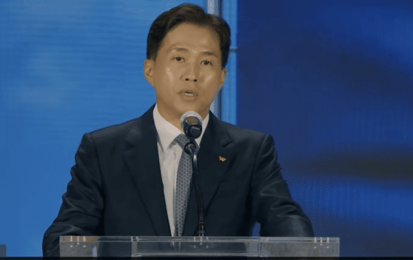
SK Hynix CEO Kwon Nak-jin put it bluntly at the ceremony. The company, he said, is “starting a new journey to shape the future of AI” from Indiana. The subtext: American AI builders will no longer have to compete for SK Hynix’s attention against Chinese firms, Japanese data centers, or even Samsung’s other clients. Their HBM supply will run through an American facility, inspected and integrated on US soil.
Why Indiana, and why this matters for the US
West Lafayette may seem an odd choice for a cutting-edge semiconductor site. It is home to Purdue University and miles from the coastal fab clusters where Taiwan’s TSMC and Intel have staked their American claims. But proximity to an engineering talent pool and a university partnership are exactly the point. SK Hynix signed a memorandum of understanding with Purdue on the same day as the groundbreaking, committing to joint research and workforce development.
The US government is already paying a share of the bill. The Commerce Department finalized a $458 million grant to SK Hynix under the CHIPS Act, bringing total public support for the project to significant levels. Indiana Governor Eric Holcomb called it the largest private development in state history. The timeline is aggressive: construction starts this October, the cleanroom is targeted for completion by October 2028, and SK Hynix plans to begin mass production of its seventh-generation HBM — codenamed HBM4E — in the third quarter of 2029.
By 2030, Kwon says the Indiana plant will be America’s primary HBM production base. That is a big claim for a facility that will not manufacture wafers. But if SK Hynix’s packaging throughput scales as expected, the claim stops sounding like marketing.
Who wins, who loses
American AI companies win immediately. Nvidia, Google, Amazon, and Microsoft all rely heavily on SK Hynix for the high-bandwidth memory that powers their training clusters. Having a packaging and testing operation on US soil means shorter logistics chains, tighter quality control, and — critically — a legal and geopolitical buffer. Export controls on advanced memory to China are tightening by the month. A US-based packaging facility makes it easier to certify that HBM destined for American clients never enters restricted supply chains.
Chinese AI builders lose the most. SK Hynix has already restricted HBM exports to Chinese customers in response to US pressure. The Indiana plant reinforces that firewall. Any HBM flowing through Indiana will carry American jurisdiction, making it politically impossible to divert to Beijing.
Samsung Electronics faces the most uncomfortable position. The South Korean rival has been slower to commit to US-based HBM packaging. Its primary US facility is a wafer fab in Taylor, Texas — focused on logic and DRAM manufacturing, not the kind of advanced heterogeneous packaging that defines the HBM value chain. Samsung’s gap is narrowing, but every quarter SK Hynix operates an American packaging line is a quarter where its clients deepen relationships that Samsung cannot easily replicate.
Intel, meanwhile, watches from both sides. It is building its own advanced packaging capabilities in Arizona and Ohio, but its memory business remains small compared to SK Hynix and Samsung. The Indiana plant does not threaten Intel directly, but it does underscore how much of the high-value memory stack has consolidated outside American ownership.
The supply chain implication that nobody is talking about
The most consequential detail in the SK Hynix announcement is also the one buried deepest: HBM wafers will be manufactured in Korea and shipped to Indiana for final packaging.
That means the single most vulnerable link in the HBM supply chain — the wafer fabrication step — remains in South Korea. Earthquakes, typhoons, or a conflict across the strait could still disrupt the flow. The Indiana plant does not solve that risk. It solves a different one: the risk that American customers cannot trust their memory supply during a geopolitical crisis.
This is a two-tier strategy. The top tier — wafer production — stays in Korea, where SK Hynix’s experience, talent, and existing infrastructure are unbeatable. The second tier — packaging, testing, final integration — moves to Indiana, where American clients can physically inspect their chips and where US export controls are easier to enforce.
The tradeoff is real. Shipping bare HBM wafers across the Pacific adds cost and lead time. But for the AI companies building clusters that require tens of thousands of HBM chips each, reliability trumps marginal savings. And as HBM demand continues to outstrip supply — especially for HBM4 and its successors — SK Hynix is effectively pre-selling capacity to its biggest customers before the plant is even built.
What happens next
The immediate consequence is a hardening of the AI memory supply chain along geopolitical fault lines. SK Hynix’s Indiana operation will serve primarily American clients. Chinese AI firms will face progressively tighter restrictions on HBM access. Japanese and European data center builders will compete for remaining capacity.
Samsung will feel pressure to accelerate its own US packaging plans. The company has not announced an equivalent facility, and industry sources say it is evaluating options. If Samsung moves slowly, it risks ceding the American market to SK Hynix at precisely the moment when US policy rewards domestic integration.
The CHIPS Act will face a stress test. The $458 million SK Hynix grant is modest compared to Intel’s multi-billion dollar asks, but it establishes a precedent: packaging is now considered strategically important enough to qualify for American subsidies. That opens the door for future applications from other memory and foundry players.
And the Purdue partnership is a quiet signal of intent. US semiconductor policy has long struggled to find workers. A university-adjacent packaging facility that trains engineers on HBM technology could become a model for how memory fabrication integrates with American education and research institutions.
SK Hynix is building more than a factory in Indiana. It is building a new layer of the AI supply chain — one that runs through American soil, serves American clients, and leaves everyone else to negotiate for the rest.