SK Hynix's Indiana Fab Is Betting on Purdue, Not Just Cornfields
SK Hynix is turning Indiana cornfields into an HBM4E fab, but the real wager isn't concrete — it's Purdue University. The partnership reveals how the AI memory race is reshaping where semiconductor power lives.
The Cornfield Isn’t the Point
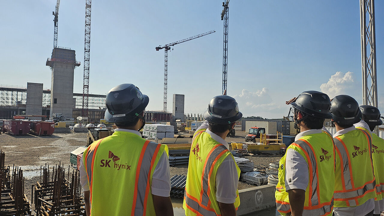
Drive south from Indianapolis Airport on Route 52 and the landscape doesn’t change for an hour — endless corn and soybean fields rolling through central Indiana. Stop in West Lafayette, a town that exists because Purdue University feeds it, and you might notice four tower cranes sticking up near campus like an accident waiting to happen.
That’s SK Hynix’s Indiana fab, currently 7 percent complete, rising out of what was, until last spring, a cornfield. The project covers 133.5 acres. The rebar alone stretches 2,635 miles — close to the diagonal width of the United States from New York to Los Angeles. The concrete poured so far could pave an eight-mile stretch of four-lane highway. When it opens, the site will employ roughly 1,000 people directly and generate an estimated 7,000 jobs across the region.
But the steel and concrete tell only half the story. The real bet SK Hynix is making isn’t in Indiana’s soil. It’s in Purdue’s labs.
The HBM Race Is Accelerating, Not Slowing
The chip SK Hynix is building here isn’t a commodity DRAM. It’s high-bandwidth memory — HBM — the kind NVIDIA, AMD, and every major AI accelerator designer is desperate for. Supply has fallen short of demand for two years running. The Indiana fab targets volume production of HBM4E by late 2029, which would be seventh-generation HBM.
Samsung Foundry has been louder about its Texas HBM ambitions and claims to have started HBM4 samples earlier. But loud announcements and volume production are different things. Samsung’s Texas fab hasn’t begun meaningful production, and its HBM roadmap has slipped publicly at least twice in the past year. SK Hynix is playing a slower, steadier game — one that bets on being right when it matters, not first.
The numbers SK Hynix gave at the April groundbreaking are vague by design. Company president Kwak Noh-jeong said the fab will produce “hundreds of thousands of DRAM wafers’ worth” of HBM annually but wouldn’t translate that into chip counts because HBM die sizes vary by generation and packaging. That evasiveness is normal for a facility that won’t ship for three years. What’s not normal is the confidence behind it.
Purdue Is the Unusual Move
SK Hynix didn’t just pick Indiana because of CHIPS Act incentives. It picked West Lafayette because Purdue sits three blocks from the construction site. The company signed a Memorandum of Understanding with the university, and the timing wasn’t accidental.
Purdue’s Birk Nanotechnology Center — an 186,000-square-foot facility funded by the Birk family endowment — houses cleanrooms, prototype fabrication equipment, and VR-based training rooms for semiconductor process learning. Professor Chun Zuhong, who is based there, says the center’s patterning tools achieve sub-10-nanometer resolution, which he explicitly linked to the capabilities needed by TSMC, Intel, and SK Hynix.
Students in full cleanroom suits work inside that facility right now. They will graduate into SK Hynix’s Indiana fab before it even produces its first wafer.
This is unusual. Samsung’s Texas fab has no equivalent university partnership of this depth. TSMC’s Arizona operation is closer to a standalone plant, staffed largely by imported talent rather than local pipelines. Intel’s Arizona expansion is similarly isolated from the regional research ecosystem. SK Hynix is doing something different: embedding its future workforce into an existing academic infrastructure while the building goes up around it.
Why This Matters Beyond Korea
The Indiana fab is a small data point in the larger fragmentation of the global semiconductor supply chain, but the direction it points is significant.
For years, memory chip manufacturing followed a simple geography: South Korea for DRAM and HBM, Japan for specialty materials, Taiwan for logic, China for assembly and testing. The US-China tech decoupling has been reshuffling that map, but most of the visible moves have been about attracting TSMC and Samsung to American soil. Few observers have tracked what SK Hynix is actually doing — a company that chose the US not just for subsidies but for the talent pipeline underneath them.
The implication is that the next phase of semiconductor competition won’t be won by who builds the biggest factory. It will be won by who can train the most engineers fast enough. HBM4E and whatever comes after it will demand process knowledge that can’t be learned from a manual. The gap between SK Hynix and its competitors may come down to whether their fabs are surrounded by universities that can feed them, or whether they’re isolated in industrial parks with nothing to draw on.
West Lafayette has Purdue. Austin, where Samsung is building, has UT Austin — but Samsung hasn’t structured anything comparable. Licking County, Ohio, where TSMC operates, has zero research universities within commuting distance. That’s not a critique of those locations; it’s a observation about what each company chose to prioritize.
Who Wins, Who Loses
SK Hynix wins if HBM4E reaches volume production on schedule in late 2029 and the Purdue pipeline delivers trained engineers in sufficient numbers. The company would solidify its position as the leading HBM supplier ahead of a generation that demands even higher bandwidth per chip — every new NVIDIA GPU will need more HBM than the last.
Samsung loses ground if it continues to miss its own timelines. The company’s HBM market share has been eroding for two consecutive quarters. Each quarter SK Hynix ships HBM4 without crisis, Samsung’s customer conversations get harder. NVIDIA and AMD are diversifying their memory suppliers precisely because they don’t want to be dependent on a single source — and Samsung’s reliability problems make that diversification easier to justify.
The region around West Lafayette wins regardless. The 7,000 projected jobs — direct and indirect — are substantial for an area whose economy has rested on agriculture and one university for decades. There are environmental concerns, as there always are with semiconductor fabs: water usage, chemical discharge, energy demand. SK Hynix has committed to minimizing those impacts, but the actual trade-offs won’t be known until the fab is running at full capacity.
What Happens Next
The next meaningful signal won’t come from a groundbreaking. It will come around mid-2028, when construction should be near completion and the first equipment installations are underway. That’s when the Purdue partnership will matter in real time — whether the university can deliver graduates with the right skills, whether SK Hynix can retain them against competitors poaching from the same pool, whether the HBM4E process itself holds up under production conditions.
If all of that goes smoothly, SK Hynix will have done something quietly strategic that the CHIPS Act narrative misses entirely: it didn’t just move a fab to America. It moved a fab into an ecosystem. That distinction will determine whether Indiana becomes a lasting node in the global memory supply chain or another expensive experiment in geographic relocation.
The cornfields are gone now. What’s growing instead will tell us everything.