LG Electronics Bypasses TSMC Bottleneck With Laser Chip Packaging Play
LG Electronics is entering the AI chip packaging equipment market with a maskless laser direct imaging system, betting that TSMC's CoWoS bottleneck will force GPU makers to diversify. The move could reshape a critical node in the semiconductor supply chain.
The bottlenecks everyone talks about
TSMC’s CoWoS (Chip-on-Wafer-on-Substrate) advanced packaging is the single most constrained step in the AI accelerator supply chain. It is not close to being solved. NVIDIA’s next-generation GPUs and a growing roster of custom ASICs from Big Tech are all funnelling through the same process, and TSMC’s expansion plans have not moved the needle enough to eliminate the shortage. The company has publicly acknowledged that the constraint will persist at least through 2027.
That gap is what LG Electronics is now targeting.
What LG actually built
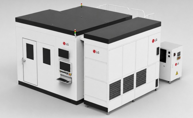
On August 21, LG’s Production Research Institute (PRI) announced its first commercial supply agreement for a maskless laser direct imaging (LDI) exposure tool. The system was developed for the fine metal interconnect step in advanced semiconductor packaging — the process that routes signals between stacked chiplets and the substrate below.
The top-spec unit patterns metal traces as narrow as 1.5 micrometres, a specification that places it squarely in the range needed for 2.1D and 2.5D organic packaging substrates. Unlike conventional stepper and scanner tools, LG’s system does not use a physical photomask. Instead, a high-precision laser beam writes circuit patterns directly onto organic interposers and high-density printed circuit boards.
The trade-off is deliberate. LG has slightly relaxed absolute resolution compared with the highest-end optical tools, then compensated by dramatically raising throughput — the amount of substrate material processed per hour. That shift in priority is significant for packaging, where speed and cost per unit matter more than hitting the resolution limits required at the front-end transistor fabrication node.
Why the no-mask approach matters
A photomask is expensive and slow to produce. A single mask for an advanced packaging layer can cost tens to hundreds of millions of Korean won and add weeks to a production run. For chiplet-based heterogeneous integration — the architecture NVIDIA, AMD, and every major cloud provider is now building around — those delays and costs multiply because each chiplet variant often requires its own mask set.
Maskless LDI eliminates that entirely. Design changes can be implemented by rewriting the laser path instead of fabricating a new mask. That is a structural advantage for the kind of low-volume, high-variety production that advanced AI packaging increasingly demands.
Who this is aimed at
The contract signed with an unnamed global OSAT (outward semiconductor assembly and test) operator marks LG’s formal entry into the B2B semiconductor equipment market. OSATs are the natural customers here. They already handle the latter stages of packaging and are under pressure to meet lead times that TSMC cannot guarantee. An equipment vendor that reduces their dependency on organic interposer and FC-BGA substrate fabrication bottlenecks is exactly who they need.
AMD and Qualcomm are the two names most likely to benefit indirectly. Both have publicly pivoted toward organic RDL-based packaging alternatives to reduce reliance on silicon interposers and TSMC’s capacity. LG’s tool is specifically optimised for that class of substrate.
What this does not mean
LG is not displacing TSMC at its own packaging lines. It is not building advanced logic dies, and it is not competing in front-end lithography at the 2-nanometre node. The play is narrower and, in some ways, sharper: supply the tooling that lets the rest of the industry build packaging capacity faster and cheaper outside TSMC’s doors.
That distinction matters. If LG were attempting to replicate TSMC’s CoWoS itself, the story would be one of sheer audacity. It is not. The company is entering a different lane of the same bottleneck — the equipment layer — and trying to widen it.
The technology is not unproven, but the commercial leap is
Maskless LDI as a concept exists. Several equipment vendors have offered LDI systems for PCB and flat-panel display manufacturing for years. What LG is doing is applying the technique to semiconductor-grade organic packaging substrates at 1.5-micrometre feature sizes — a step up in both the precision demanded and the materials being patterned. Moving from display equipment to semiconductor packaging equipment is a non-trivial climb in qualification cycles, defect-control discipline, and customer trust.
The signed contract with a major OSAT is a real signal. It is also only the first. Semiconductor equipment sales cycle length and yield爬坡 periods typically stretch across multiple quarters. Translation: this is a credible start, not a completed breakthrough.
The bigger strategic arc
This move fits a wider pattern at LG. The company’s PRI division has spent years internalising precision laser and optical technology through its work on LG Display’s OLED manufacturing equipment and LG Energy Solution’s battery electrode and assembly tools. The knowledge was always there; the market application is simply expanding beyond consumer electronics and automotive batteries into semiconductor infrastructure.
Under the direction of LG Electronics president Cho Ju-wan, the group has been pushing to extend its B2B smart-factory and manufacturing-equipment business beyond its current footprint. Entering the semiconductor equipment market as a sole-source vendor for LDI packaging tools is a concrete version of that strategy — and one that carries far higher margins and strategic positioning than most of LG’s existing industrial-equipment businesses.
What happens next
If LG’s LDI tools gain traction with OSATs over the next 12 to 18 months, two things follow. First, organic-interposer-based packaging capacity outside TSMC expands faster than it otherwise would. Second, TSMC’s CoWoS advantage becomes slightly less of a choke point — not because TSMC loses capability, but because the alternative widens enough to lower the premium on waiting in line.
For NVIDIA, AMD, and the Big Tech ASIC builders, the upside is obvious: more packaging options, shorter lead times, and less single-vendor risk at the most critical step in the AI chip supply chain. For TSMC, the implication is more subtle but real: a growing share of advanced packaging work migration to non-TSMC OSAT lines, powered in part by equipment LG sells.
For LG, the payoff depends on execution. One signed contract is a starting line. Scaling it into repeated orders, qualifying additional OSAT customers, and maintaining yield at 1.5 micrometres across thousands of substrates per month is where the real test begins. If it clears that bar, LG Electronics stops being remembered only as a home-appliance and display maker — and starts functioning as a semiconductor-equipment supplier with genuine leverage in one of the world’s tightest supply chains.
The maskless laser may be a small tool. In the current packaging bottleneck, it could turn out to be an outsized one.