Memory Is Eating GPUs. Samsung and SK Hynix Are Betraying That Shift
At Hot Chips 2026, Samsung and SK Hynix unveiled opposing strategies to turn HBM from a passive storage component into an active processing unit. The implications for NVIDIA, TSMC, and the entire AI hardware supply chain are enormous.
The Memory Wall Just Got Personal
For decades, the semiconductor hierarchy was clear. GPUs computed. Memory stored. The boundary was architectural dogma, reinforced by every textbook and every product roadmap.
That hierarchy is collapsing at Stanford. At Hot Chips 2026, the two Korean memory giants — Samsung and SK Hynix — presented not incremental upgrades but a philosophical rupture: HBM (High Bandwidth Memory) is no longer a passive component waiting for instructions. It is becoming a participant in computation itself.
The reason is brutal and familiar. GPU performance has outpaced memory bandwidth for years. The “memory wall” — the gap between how fast a processor can compute and how fast it can be fed data — has become the single most constraining bottleneck in AI training and inference. Every generation of more powerful chips makes this worse, not better. The solution, as both Korean firms are now betting, is not to build faster GPUs but to make memory smarter and closer.
Samsung Is Rewriting the Base Die
Samsung’s pitch was the more ambitious of the two presentations. Han Sang-wook, Samsung’s technical leader, described a three-stage roadmap that effectively dissolves the boundary between memory and logic.
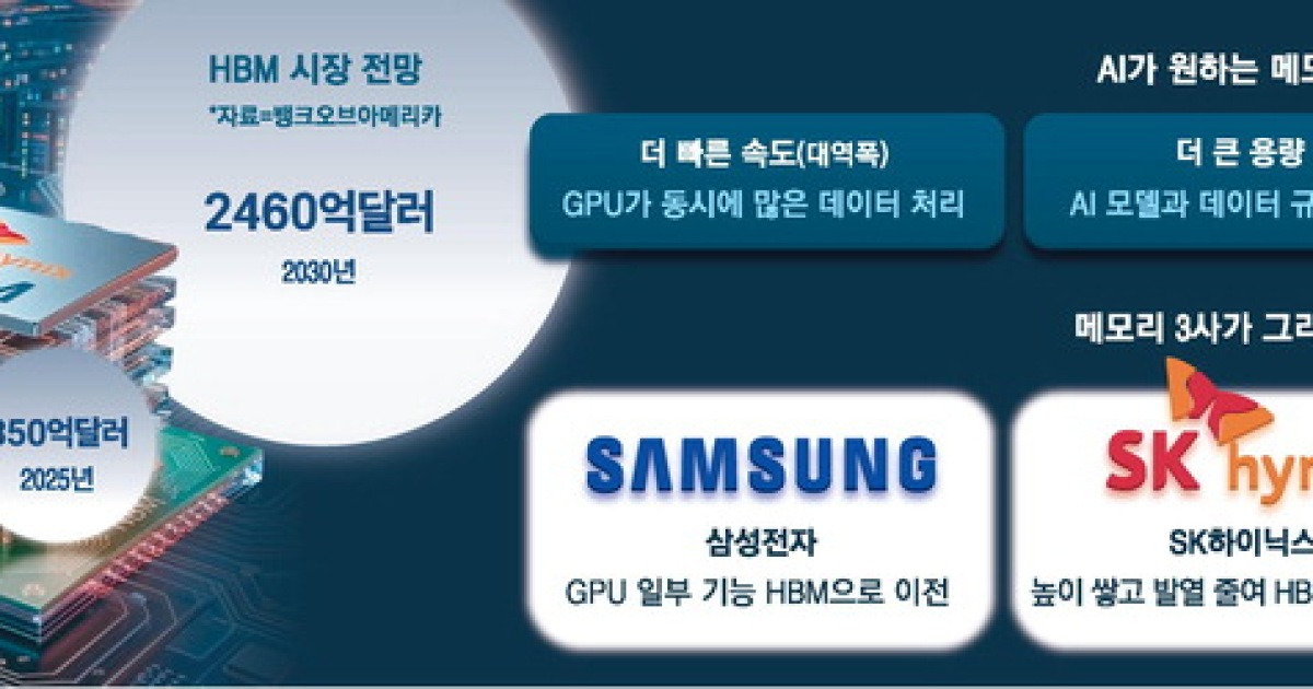
The first stage targets what has always been the most useless part of an HBM stack: the base die at the bottom, which currently serves only as a data pathway between the memory layers and the outside world. Samsung plans to fabricate that base die using advanced logic process technology — the same kind of fabs that build processors — turning it into what Han called a “small brain.” GPU-level memory management functions would migrate into HBM itself, freeing the main GPU to focus exclusively on computation.
The second stage is zHBM: stacking that smart base die directly on top of the GPU, fusing memory and processor into a single physical package. The third stage extends that integration further.
The claimed savings are dramatic. Samsung estimates zHBM could reduce power consumption by roughly 70 percent compared to the forthcoming HBM5 standard. That is not an efficiency tweak. It is an order-of-magnitude improvement in a domain where power density is already a critical constraint.
Samsung can do this because it is one of the very few companies on Earth that designs DRAM, manufactures it, and operates a leading-edge foundry — all under one roof. The base die does not need to be outsourced. The company can draw the entire architecture internally.
This matters beyond Samsung’s balance sheet. If HBM becomes a programmable substrate rather than a commodity part, the customer relationships that define the semiconductor industry shift fundamentally. Memory suppliers will need to co-design with GPU makers from day one. NVIDIA, AMD, and Intel’s own AI divisions will no longer be buying components; they will be co-authoring systems.
SK Hynix Chooses Packaging Over Architecture
SK Hynix took a different path — one shaped by the structural handicap it shares with almost every fabless company: it does not control advanced logic fabrication. SK Hynix sends its leading-edge logic work to TSMC. That means it cannot easily redesign the base die the way Samsung can.
Instead, SK Hynix is doubling down on what it already does best: packaging. Lee Jae-sik, SK Hynix’s vice president of American operations, emphasized two technologies. The first is hybrid bonding capable of stacking more than 20 layers of DRAM — a significant step up from the 12-to-16-layer stacks that currently dominate production. The second is i-HBM, a targeted cooling system that channels refrigeration precisely where heat concentrates rather than cooling the entire package uniformly.
The strategy is pragmatic. Rather than redesigning the chip’s internal architecture, SK Hynix is making the existing architecture denser and thermally viable. It is the engineering equivalent of building a taller, better-cooled building instead of inventing a new foundation.
The limitation is also clear. SK Hynix’s approach preserves the traditional separation between memory and logic. It improves bandwidth and thermal efficiency without challenging the underlying model of what an HBM stack is for. Samsung’s approach, for all its ambition, is the one that redefines the category.
Even Buyers Are Designing Now
Perhaps the most consequential moment at Hot Chips was not about Korean memory makers at all. Meta, in collaboration with AI chip startup DMatric, revealed a “3D DRAM” prototype: custom-designed DRAM stacked directly beneath a compute chip, fabricated as a single monolithic unit rather than assembled through conventional packaging.
The numbers are striking. Meta claims the approach reduces data-movement power to one-sixth of what HBM consumes and pushes bandwidth to 100 terabytes per second. The design philosophy is the same as Samsung’s — shrink the distance data travels, accept that off-the-shelf memory is no longer good enough — but the actor is different. This is a buyer, not a supplier, choosing to engineer its own memory architecture.
That Meta, Amazon, Google, and Microsoft are all beginning to design custom memory structures for their own AI clusters signals a structural change in the industry. The commodity memory market — where buyers specified a part number and sourced it from whoever could deliver — is retreating. Custom memory co-design is becoming the default for anyone serious about AI performance.
The Money Problem, Not the Technology Problem
Jim Handy of Objective Analytics put it plainly at the conference: the 2026 memory bottleneck is not a technology problem. It is a capital problem. Demand for HBM has surged alongside AI investment, but production capacity has not kept pace. Price and supply constraints have become the binding bottleneck, not lithography or circuit design.
Handy’s diagnosis suggests the race between Samsung and SK Hynix is as much about who can scale production as who can innovate. A 70 percent power reduction means nothing if you cannot ship enough units to matter. A 20-layer stack is impressive until a competitor ships 18 layers at half the price with a six-month lead.
The capital intensity of this competition is also rising. Samsung’s roadmap requires advances in both memory fabrication and logic-process base dies. SK Hynix’s requires sophisticated bonding and cooling infrastructure. Meta’s custom memory effort requires its own design capabilities and fab partnerships. Every player is moving toward higher fixed costs and deeper vertical integration.
Who Wins, Who Loses, What Comes Next
The immediate winner is the company that gets the first widely adopted custom-memory AI system. Samsung has the structural advantage — it can do everything in-house — but Samsung’s foundry business is not yet competitive with TSMC’s at the most advanced nodes. SK Hynix has the packaging leadership but depends on TSMC for logic. Neither can unilaterally dictate the next generation of AI hardware.
NVIDIA is the likely loser in the short term if this trend accelerates. The company’s moat has rested partly on controlling the GPU ecosystem and treating memory as a specification to be met, not a variable to be designed. If memory becomes a differentiating architecture rather than a commoditized input, NVIDIA’s bundling advantage narrows. The company will respond — it always does — but the dynamics have shifted.
TSMC occupies an ambiguous position. It is the essential fab for SK Hynix’s logic needs and for many AI chip designers. But if memory manufacturers like Samsung begin integrating logic and memory fabrication more deeply, TSMC’s role as the unavoidable intermediary shrinks. TSMC’sCoWoS packaging business benefits from the current architecture. A future where memory and logic are monolithically fabricated challenges that model too.
The Korean companies themselves face a risk they may not fully appreciate. The convergence of memory and logic is historically the domain of companies like Intel and Samsung, both of whom have struggled in recent years to translate vertical integration into sustainable competitive advantage. Integration is not optimization. A company that builds everything can also build everything poorly.
What is certain is that the era of off-the-shelf HBM is ending. The companies that treat memory as a design parameter rather than a purchase order will define the next generation of AI hardware. The ones that do not will be specifying someone else’s architecture.