Samsung's ASML Bet to Lock In DRAM Supremacy
Samsung is co-developing 12-inch photomasks with ASML alongside High NA EUV equipment, a move designed to secure first-mover advantage in next-gen DRAM by 2028—and widen the gap with SK Hynix.
Samsung isn’t just buying ASML’s most expensive tool. It’s trying to own the ecosystem around it.
When Samsung announced a deeper partnership with ASML that extends beyond High NA EUV equipment into 12-inch photomask co-development, the move looked like procurement strategy at first glance. The real play is far more ambitious: Samsung is attempting to lock in the architectural standards for next-generation DRAM before its rivals can catch up.
The timing is everything. High NA EUV tools begin mass production deployment in 2028. That is the year Samsung wants to be the first company to ship AI-grade DRAM built on that platform. If it succeeds, the gap between Samsung and SK Hynix—the two giants controlling the bulk of global memory chip output—widens materially. If it stalls, the entire bet loses its edge.
Why 12-inch photomasks change the calculus
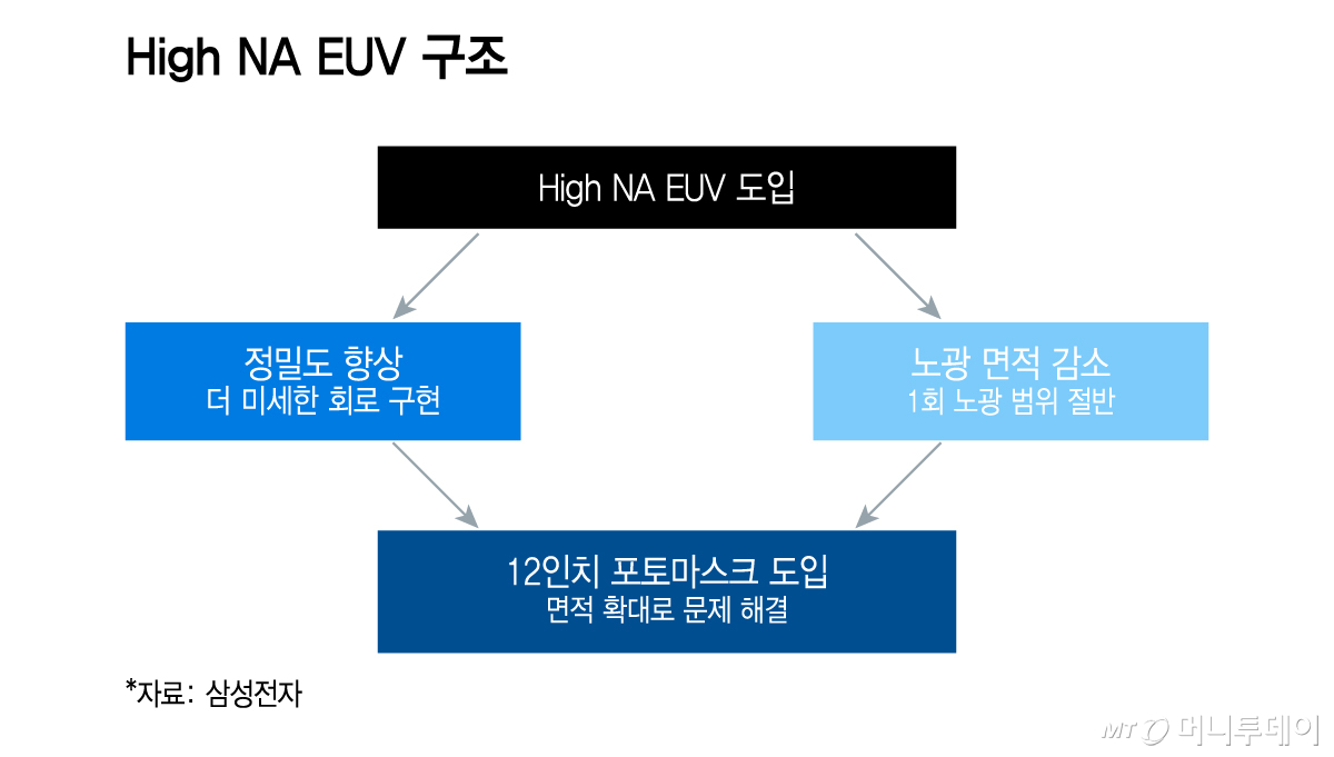
High NA EUV prints circuit features down to roughly 8 nanometers, compared to about 13 nanometers on current EUV tools. The trade-off is brutal: the area you can expose in a single shot shrinks by half. For a DRAM chip, that means you currently would need to stitch multiple smaller patterns together, layer by layer, to build the final die. Each stitching operation introduces alignment error risk. Each error costs yield. Yield kills margins.
The 12-inch photomask solution flips that problem. Instead of using a 6-inch mask and tiling the pattern across the wafer multiple times, a single 12-inch mask exposes a much larger area at once. You cut the number of stitching operations roughly in half. Fewer stitches mean fewer defects, higher throughput, and a shot at producing AI-grade memory at volumes that actually matter for margin.
Samsung is not waiting for ASML to solve this alone. It is co-developing the mask with ASML from the ground up. That is unusual. Equipment makers typically hand off tool specifications to fab operators and let the fabs figure out the rest. Samsung is instead inserting itself into the standard-setting phase.
If the 12-inch mask becomes the de facto specification for High NA EUV production, Samsung writes part of the code. Every other fab that follows will be reading from the same playbook. That is how you turn a equipment purchase into a structural advantage.
Who loses if Samsung pulls this off
SK Hynix is the obvious answer, and the competitive math favors Samsung here. SK Hynix already leads in HBM—High Bandwidth Memory—the specialized DRAM that AI data centers demand. But HBM sits in a different lane from mainstream DRAM. The High NA EUV push targets the broader memory ecosystem: the commodity-grade chips that power everything from smartphones to servers. If Samsung captures first-mover advantage on that front, it controls the cost curve for the next generation of mainstream memory.
TSMC is the second loser, though in a different way. ASML supplies High NA EUV tools to TSMC and Intel as well. But those customers are foundries—they design chips for other companies. Samsung is both a memory maker and a foundry operator. The process know-how Samsung builds with ASML on High NA EUV for DRAM production transfers directly to its foundry division. That means Samsung can offer AI chip manufacturers a process node that benefits from the same ecosystem investment that its own DRAM business helped fund. TSMC does not get that crossover.
Intel, paradoxically, may also find itself behind. The company is betting heavily on its own foundry ambitions and has struggled to keep pace with both Samsung and TSMC on leading-edge lithography timelines. If Samsung and ASML lock in a production standard that Intel cannot easily adopt without retrofitting its own tooling, the gap grows.
What the numbers actually mean
Samsung claims the High NA EUV platform can shrink individual transistors by up to 1.7 times and increase density by up to 2.9 times compared with current EUV. Those are theoretical maximums. Real-world yield improvements will matter far more than the headline ratios.
Samsung began using EUV for DRAM production in 2020—the first company to do so. That earlier bet paid off: Samsung now produces a significant share of global DRAM with EUV techniques, and its yield on those lines is considered industry-leading. The High NA EUV timeline mirrors that pattern. Samsung is not experimenting with unproven equipment. It is deploying the next evolution of a platform it already dominates.
The 2028 mass production target is aggressive but not impossible. ASML has been shipping High NA EUV tools since 2024, and the company has reported steady improvement in tool uptime and output. The bottleneck is not the equipment itself—it is the surrounding ecosystem: masks, resists, metrology, and process integration. That is exactly why Samsung is co-developing the 12-inch mask with ASML rather than waiting for suppliers to catch up on their own timeline.
Why this matters beyond Korea
South Korean outlets are treating this as a domestic industry story. The real significance is global. The AI infrastructure buildout is consuming memory at a rate that did not exist five years ago. Data centers need DRAM not just in volume but at ever-higher densities. Every point of yield improvement on the leading edge translates into millions of additional chips available for AI training and inference workloads.
Samsung’s move is a supply-chain power play disguised as a technical partnership. By securing access to High NA EUV and shaping the photomask standard simultaneously, Samsung is positioning itself as the gatekeeper for the next generation of memory production. If it succeeds, the company does not just win market share—it wins the right to define what “next-generation DRAM” means.
The question is whether ASML will allow one customer to capture this much of the value chain. The company supplies tools to multiple foundries and memory makers. But Samsung’s dual role as both memory producer and foundry operator gives it an incentive and a capability that no single-purpose competitor matches. That asymmetry is the entire point of the bet.
What happens next
Watch for three indicators over the next 18 months. First: whether Samsung and ASML announce formal 12-inch photomask qualification milestones. Second: whether SK Hynix responds with its own mask or equipment partnerships, or chooses to wait and observe. Third: whether TSMC and Intel adjust their High NA EUV adoption timelines in response to Samsung’s head start.
If Samsung hits its 2028 target with clean yields, the DRAM market reconfigures around a company that already controls the lithography standard. If it stumbles, the advantage evaporates quickly—because every competitor in this space has the same ASML tools and the same roadmap. The difference is who moves first and who builds the ecosystem around the technology.
Samsung is betting that speed and integration beat isolation. In memory semiconductor competition, that has been the winning formula for decades. The High NA EUV era could be the moment it pays off again.