SK Hynix Bets on Hybrid Bonding to Defend HBM Throne
SK Hynix is deploying two experimental hybrid-bonder lines at Cheongju — one domestic, two foreign — to leapfrog past bump-limited stacking into 20-layer HBM5 by 2028. The move reshapes the race against Samsung and tightens AI-accelerator supply chains.
The move most people missed
SK Hynix quietly shipped two hybrid-bonder prototypes into its Cheongju fab last quarter. They are not yet running production lines. But once they do — likely sometime in 2028 when eighth-generation HBM5 enters volume manufacturing — they will mark the first major packaging-level upgrade to HBM stacking in five years.
The hardware is unusual in how it was sourced. One tool came from Hanwha Semitech, a domestic Korean equipment maker. The other two came from Valsi in the Netherlands and Applied Materials in the United States. SK Hynix is not betting on a single vendor. It is simultaneously qualifying three process routes, each feeding the same test line, in what amounts to a deliberate dueling-strategy designed to lock in yield and reliability before any single supplier can become a bottleneck.
What makes this particularly notable is that Hanwha Semitech’s participation signals a broader push within Korea to localize advanced packaging equipment — an effort accelerated by export controls and the geopolitical friction surrounding semiconductor supply chains. If Hanwha’s platform proves viable alongside its foreign counterparts, it could fundamentally shift the economics of HBM production away from imported capital equipment toward a more resilient domestic ecosystem.
Why hybrid bonding matters more than you think
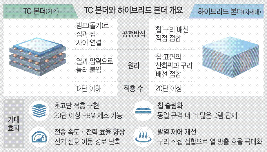
Current HBM uses thermal-compression bonding — a technique that squeezes tiny solder or copper bumps between stacked DRAM dies and fuses them with heat and pressure. As SK Hynix itself has explained in earlier patent disclosures, bump-based stacking hits a hard wall: every additional layer adds height, widens the I/O pitch, increases thermal cross-talk, and drags down electrical performance. That is why the current market cap for HBM sits at roughly 12 layers. Stacking beyond that becomes economically brutal.
Hybrid bonding removes the bumps entirely. It aligns copper microvias on adjacent die surfaces and bonds them directly at the atomic level. The result is a thinner interconnect, shorter signal paths, lower power per bit transferred, and higher bandwidth per package. For SK Hynix, the immediate prize is enabling stacks of 16, 20 or even more layers inside the same physical envelope — without demanding proportionally larger PCB real estate or heavier cooling.
In practical terms, a 20-layer HBM5 package built with hybrid bonding could deliver significantly more aggregate bandwidth than a 12-layer HBM4 today while consuming less energy per terabyte moved. That gap is what NVIDIA and AMD are racing to close in their own GPU architectures, because HBM capacity and bandwidth directly dictate how fast those accelerators compute.
The competitive stakes
Samsung Electronics currently holds a narrow lead in HBM share, driven largely by its ability to scale bump-bonded HBM4 quickly after TSMC’s CoWoS packaging constraints tightened in 2024. SK Hynix’s hybrid-bonding pivot is therefore both a technological bet and a strategic counterpunch. If Cheongju achieves reliable 20-layer throughput by 2028, Samsung’s bump-bonding advantage erodes precisely where it matters most — in the ultra-high-density configurations that next-generation AI trainers demand.
But Samsung is not idle. Industry sources indicate the company has initiated internal evaluations of direct-copper hybrid bonding, though no prototype equipment orders have been confirmed. This creates a window in which SK Hynix could extend its first-mover lead by 12 to 18 months if it manages to qualify its multi-vendor line faster than Samsung closes the gap. The dueling strategy itself is a hedge: should Valsi’s European equipment face export-licence delays, or should Applied Materials encounter U.S.-Korea compliance friction, Hanwha’s domestic alternative keeps the experiment moving.
Supply-chain ripple effects
The implications stretch well beyond Cheongju. TSMC’s CoWoS capacity remains the binding constraint on the entire AI accelerator pipeline, and every extra bit of HBM density that SK Hynix can ship from its own domestic lines reduces reliance on overseas packaging. This matters because TSMC’s queue lengths have already forced some memory vendors to consider alternative routing through Intel Foundry or domestic Korean packaging houses. Hybrid bonding, if it matures, gives SK Hynix a path to increase bandwidth-per-package without requiring proportional increases in co-packaging footprint — effectively decoupling HBM density growth from TSMC’s availability.
For equipment suppliers, the divergence is equally significant. Valsi stands to gain substantial revenue from hybrid-bonder sales across multiple clients, not just SK Hynix. Applied Materials’ entry reinforces its position in advanced packaging metrology and surface preparation. Hanwha Semitech’s inclusion represents a potential inflection point for a company traditionally focused on legacy process equipment — success here could reposition it as a full-spectrum packaging supplier. Conversely, companies whose revenue models depend on thermal-compression bonder maintenance contracts face structural headwinds as the industry shifts architecture.
Secondary effects are already visible in hiring patterns. SK Hynix has expanded its Cheongju packaging R&D headcount by approximately 30 percent over the past year, pulling talent from Samsung and global foundries. This recruitment war drives up labor costs across the sector but also accelerates knowledge transfer that benefits the broader Korean ecosystem.
What analysts are watching
Bloomberg Intelligence and TrendForce both flagged the Cheongju shipments in recent notes, though neither has revised near-term revenue models aggressively. The consensus view is cautious: hybrid bonding is promising but unproven at volume, and yield rates on direct-copper alignment remain poorly disclosed. Failure modes — particularly microvia misalignment and contamination during surface-prep — could delay commercialization by a year or more. Even under optimistic scenarios, 2028 volume assumes no catastrophic equipment failure and stable export-regime conditions through the qualification phase.
What would change the calculation dramatically is early customer feedback. If NVIDIA or AMD signs design-win letters tied to SK Hynix’s hybrid-bonded HBM5 before 2027, the market would likely re-rate the stock significantly upward. Absent that signal, the project remains an expensive research program with uncertain payoff. Either way, SK Hynix has made clear it will not wait passively for competitors to define the next HBM generation.
The close
SK Hynix is not simply upgrading a packaging tool. It is restructuring the economics of HBM scaling itself — trading bump-dependent density gains for a direct-bonding approach that promises more layers, less power, and greater independence from foreign packaging capacity. Whether that gamble pays off depends on execution over the next two years, the stability of its multi-vendor equipment strategy, and whether AI demand continues its current trajectory long enough for the investment to mature. The Cheongju fabs will tell.