SK Hynix's Indiana Gambit: The 'Made in USA' HBM Strategy
SK Hynix is building the first 'Made in USA' HBM packaging facility in Indiana, signing a deal with Purdue University and projecting 7,000 jobs. The move reshapes the AI chip supply chain and locks in Seoul's strategic leverage.
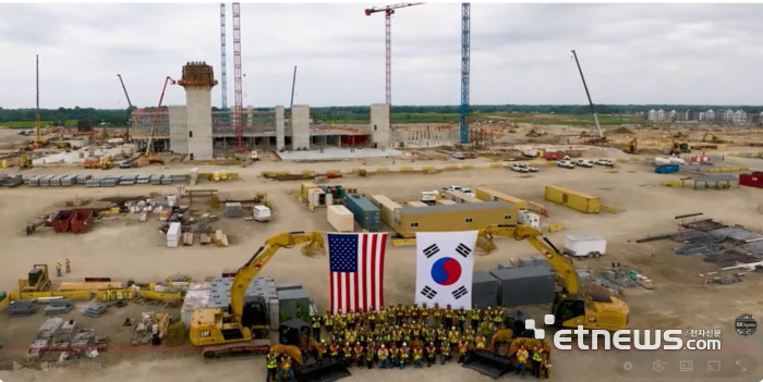
The First ‘Made in USA’ HBM Base Takes Shape in Indiana
SK Hynix is building the first advanced packaging facility in the United States dedicated to high-bandwidth memory — the fastest, most expensive chips in the AI stack. On August 27, the company broke ground at Purdue University in West Lafayette, Indiana, in a ceremony that read like a who’s-who of the American semiconductor establishment: Governor Mike Braun, Senator Todd Young, Purdue President Mitch Daniels, and South Korea’s ambassador to the US, Kang Kyung-wha. The message was deliberate. SK Hynix wants the world to know this is not just another factory. It is the anchor of a new supply chain axis.
Why HBM Packaging Matters More Than You Think
High-bandwidth memory is not commodity DRAM. It is the memory that sits next to GPUs inside AI servers, shipping data at rates that determine whether a model trains overnight or next week. SK Hynix dominates this market. It supplies HBM to Nvidia, AMD, and Intel’s Foundry division. But dominance comes under pressure.
The CHIPS Act creates subsidies for US-based production. The Biden administration has made clear that allied nations should not rely on a single geography for critical components. China is building its own memory capacity. Samsung’s Indiana fab has been slower to materialize than promised. Every month without a US-based advanced packaging line is a month where Washington looks the other way as competitors encroach.
SK Hynix saw the opening. Its Indiana facility will handle advanced packaging — the process of stacking HBM chips and connecting them to logic dies. Packaging is where the highest value is captured, and where supply chain vulnerabilities concentrate. A single damaged interconnect can scrap an entire HBM module worth thousands of dollars.
The Purdue Partnership: More Than a Photo Opportunity
The ceremony included a memorandum of understanding with Purdue University for R&D collaboration in advanced packaging. This is not ceremonial. Purdue operates the Bucky Nano Technology Center, one of the few US research facilities with deep expertise in semiconductor packaging. The university produces engineers in high numbers. The proximity of the lab to the fab is the difference between hiring from a limited local pool and building a sustainable talent pipeline.
The Indiana Economic Development Corporation, the state agency overseeing the project, has projected over 7,000 direct and indirect jobs during construction and operation. That is a significant number for a rural industrial zone, and it gives the project political insulation. Any future administration that considers revoking CHIPS subsidies would face a constituency of thousands of workers and hundreds of supplier companies.
More than 100 materials, components, and equipment suppliers are currently discussing relocation to West Lafayette. That supply chain density is what turns a single factory into an ecosystem. It is also what makes the facility harder to displace.
The Strategic Calculus: Why This Lands Where It Does
SK Hynix is playing a three-board game. In America, it is positioning itself as indispensable to the US AI strategy — a supplier that can deliver “Made in USA” HBM for AI accelerators, satisfying procurement requirements that increasingly favor allied-origin components. In Korea, it is demonstrating that Seoul can deliver economic growth without capitulating to Chinese demands for technology transfers that would erode its competitive edge. Globally, it is forcing Samsung to respond or risk ceding the US packaging lead.
Samsung’s Tayo Fab in Taylor, Texas, is a broader semiconductor complex. It has not committed to HBM packaging at scale. SK Hynix is exploiting that gap. The company’s CEO, Kwak Noh-jeong, said at the ceremony that Indiana would become the first base to provide “Made in USA” HBM. That claim is about to be tested — but the announcement alone shifts the narrative.
What Loses and What Wins
Who wins: SK Hynix. It gains access to CHIPS Act subsidies, a political ally in Indiana’s congressional delegation, and a first-mover position in US-based advanced packaging. It also strengthens its relationship with American AI customers who face increasing pressure to source from allied supply chains.
Who loses: Samsung. It now faces a competitor with a credible US packaging story. The company must accelerate its own plans or risk losing US-based customers to SK Hynix’s supply chain advantages. There is also the question of whether Samsung’s existing HBM fabs in South Korea remain sufficient, or whether Washington will begin questioning the reliability of memory sourced entirely from abroad.
The broader loser is China. US-based HBM packaging reduces the leverage Beijing could have gained by restricting material exports or targeting Korean fabs with economic pressure. If the US holds the packaging step, it holds a chokepoint in the AI supply chain that China cannot easily replicate.
The Timeline and the Risk
Groundbreaking does not mean production. The facility will take years to complete. Equipment qualification, workforce training, and yield ramp — the last two being the hardest — typically add further delays. SK Hynix will need to prove it can deliver HBM at the quality levels it maintains in Korea, and do so from an American site that has never produced this class of memory.
There is also the question of subsidy certainty. CHIPS Act funding has faced legislative headwinds. If Washington pulls back, the economic calculus changes. But the 7,000-job projection and the 100+ supplier ecosystem create a constituency that makes cancellation politically expensive.
The Bigger Picture: Memory as Geopolitics
The Indiana facility represents a shift in how memory — once the most globalized, commoditized segment of the semiconductor industry — is being redefined as a strategic asset. SK Hynix is not just building a factory. It is rebuilding the assumption that advanced memory must flow across oceans from a single geography. The company is making the case that it can produce the same chips, with the same performance, from American soil.
If that case holds, the implications extend well beyond Indiana. They reshape how Washington thinks about supply chain resilience. They reshape how Seoul positions itself as a technology ally. And they reshape the competitive dynamics between the world’s two largest memory makers.
The ceremony at Purdue was small in physical scale compared to the fabs it references. But the ambitions behind it are enormous. The first “Made in USA” HBM is not yet a product. It is a promise. Whether that promise becomes a supply chain advantage or a costly delay will define the next chapter of the AI chip war.