SK Hynix Bets Its AI-Memory Future on TSMC's Ecosystem — and the Geopolitics That Follows
SK Hynix unveiled its full next-gen HBM portfolio at TSMC's Open Innovation Platform conference in Santa Clara, pairing HBM4 with NVIDIA's Vera Rubin superchip and validating HBM5 on TSMC's CoWoS packaging. The move signals a deeper strategic lock-in with the US-Taiwan AI supply chain, reshaping how Korea's chipmakers navigate export controls.
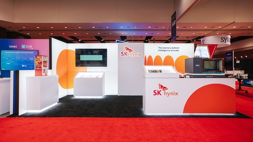
A Santa Clara Booth Tells a Bigger Story Than a Product Lineup
The unglamorous detail buried in a Yonhap News TV report this week is the most consequential one: SK Hynix has been attending TSMC’s Open Innovation Platform (OIP) conference every year since 2024, and this September, it came to the Santa Clara edition with its entire next-generation AI memory stack on display.
That cadence matters more than the product slides. A single booth appearance at a foundry’s industry event is routine. A multi-year, recurring presence at the open-innovation arm of the world’s largest contract chipmaker is a structural commitment. It means SK Hynix is not just selling memory to TSMC’s customers; it is co-developing packaging, validating roadmaps, and embedding itself in the TSMC-NVIDIA design cycle before a single production wafer ships.
The Vera Rubin Connection and Why It Locks in SK Hynix
At the Sept. 23 conference, SK Hynix paired its HBM4 — the sixth-generation high-bandwidth memory, in a 36 GB, 12-stack configuration — with NVIDIA’s upcoming “Vera Rubin” AI superchip. That product pairing was not a footnote. It was the centerpiece of the booth, under the slogan “Memory Supporting Large-Scale AI Expansion.”
For an international reader unfamiliar with the Korean chip landscape, the stakes here are easy to understate. SK Hynix and Samsung have spent three years in a brutal HBM race, both trying to be the default memory supplier for NVIDIA’s GPU roadmap. Samsung lost ground badly in the HBM3E cycle after quality issues with its early samples. SK Hynix recovered, and by anchoring HBM4 directly to Vera Rubin in a public, TSMC-co-sponsored setting, it is effectively telling the market: when NVIDIA’s next superchip spins out of TSMC’s fabs, the memory that rides on top of it will carry SK Hynix’s logo.
The surrounding product family tells the same story. Alongside the HBM4, SK Hynix displayed its seventh-generation HBM4E in a 48 GB, 12-stack form, a 48 GB, 16-stack variant of HBM4, and its existing HBM3E line. Then there was the 96 GB SOCAMM 2 module and a 192 GB SOCAMM 2 physical unit — server main-memory products that extend SK Hynix’s reach beyond the GPU board into the CPU socket and the rack-level memory pool that every AI data-center build now requires.
CoWoS Validation Is the Real Moat
The award that will draw the most quiet attention is the “Partner of the Year” prize in TSMC’s 3DFabric-HBM Integration category, which SK Hynix took for the second consecutive year. TSMC cited the company’s collaborative work validating HBM5 — the eighth generation, a product that will not ship for another two to three years — using TSMC’s CoWoS (Chip-on-Wafer-on-Substrate) advanced packaging.
This is where the strategic logic clicks. HBM5 will not be a drop-in replacement for HBM4. It will require tighter co-design between the memory die stack and the interposer or substrate that TSMC fabricates. A foundry that has been testing a foundry partner’s HBM5 on its own packaging line for a full year ahead of schedule is building a joint engineering moat that a competitor cannot replicate without starting that clock over.
Samsung, for its part, has its own HBM5 roadmap, but the public record of a TSMC-validated HBM5 test loop does not yet show Samsung in the same seat. Whether that gap closes by 2027 depends on internal timelines neither company will disclose. What is public is the sequence: SK Hynix went first, and it did so on TSMC’s own packaging platform.
The Geopolitical Undercurrent Most Readers Will Miss
Here is the layer that a Seoul-based business report and a Taipei-based trade newsletter will both half-catch but few English-language outlets will connect: SK Hynix staging its HBM debut in Santa Clara, on TSMC’s turf, during a TSMC-hosted event, is a deliberate signal to Washington.
The United States has imposed successive export controls restricting the flow of advanced AI chips and the lithography tools needed to make them to China. Memory chips, particularly HBM, sit squarely inside the technology stack those rules police. A Korean memory vendor that is publicly co-engineering its next three HBM generations on a Taiwanese foundry’s packaging line, in a US city, at a US-based conference, is building a paper trail that makes it harder for any future administration to argue that Korea’s HBM output is a free-standing export channel to restricted markets. The ecosystem integration itself becomes a compliance asset.
It also reduces SK Hynix’s vulnerability to a single-point regulatory shock. If the US tightened rules on HBM4 or HBM5 shipments, a SK Hynix that is deeply embedded in TSMC’s US and Arizona production chains — where TSMC is building a $65 billion fab complex in Phoenix — can argue for treatment as a node in a US-aligned supply chain rather than an independent Korean exporter subject to separate licensing regimes.
The SSD Chiplet Bet Worth Watching
Less heralded in the source material but strategically significant: SK Hynix said it is preparing chiplet-based SSD solutions for the sixth and seventh generations of its enterprise PCIe solid-state drive line, tied to the expected growth in AI-infrastructure storage. Chiplets for SSDs mean disaggregating the controller and NAND packages onto a shared substrate, a technique borrowed from HBM and advanced logic packaging. If SK Hynix pulls that off, it extends the same co-design advantage it has built in HBM into the storage tier, where Western Digital and Kioxia currently hold strong positions.
Who Wins, Who Loses, What Comes Next
The short-term winner is clearly SK Hynix: a public reaffirmation of its NVIDIA partnership, a second-year TSMC award, and a product family that spans HBM3E through HBM5 plus SOCAMM 2 and eSSD. The medium-term winner is TSMC itself, which gains a committed HBM partner validated on CoWoS, strengthening its integrated-package pitch against Intel’s Foveros and Samsung’s in-house foundry ambitions.
The loser, if you must name one, is Samsung. It is not being publicly excluded, but the optics of a Korean rival winning a two-year partner streak at a TSMC event while Samsung pushes its own HBM4 and HBM5 roadmaps on its own foundry packaging creates a perception gap in analyst models and investor sentiment that will be hard to close before the next earnings season.
What happens next is procedural: SK Hynix will continue its annual OIP appearances, likely returning to Santa Clara or a TSMC venue in Hsinchu in September 2027. The HBM5-to-HBM5E transition will determine whether the partner-award streak extends. And the Vera Rubin superchip, wherever it lands in NVIDIA’s revised 2027 launch timeline, will be the product that finally puts SK Hynix’s 36 GB HBM4 stack in enough data centers for the number to stop being a spec-sheet figure and start moving equity prices in Seoul.