Korea Challenges Japan in the Race for Next-Gen Chip Packaging
Samsung Electro-Mechanics and LG Innotek are moving into Intel's EMIB-T substrate supply chain, directly challenging Japanese leader Ibiden. The shift could redraw semiconductor packaging power dynamics if Seoul succeeds where Tokyo has dominated for nearly a decade.
The Substrate Gambit
Two months ago, Intel quietly opened its EMIB-T packaging technology to external suppliers. It had guarded that capability exclusively for its own chips for years. Now Google is confirming it will use EMIB-T in its next-generation TPU accelerator launching in late 2027. And from across the sea, two Korean firms — Samsung Electro-Mechanics and LG Innotek — are racing to get their names on the supply chain.
This is not a trivial pivot. Advanced packaging substrates sit at the bottleneck of the AI chip boom. As chip designers struggle to shrink transistor nodes for marginal gains, the real performance leaps are coming from connecting multiple dies together efficiently. The substrate that makes that connection possible has become a strategic chokepoint — and right now, nearly all of it flows through Japan.
How EMIB-T Changed the Math
To understand why this matters, you need to understand what EMIB actually does. Modern AI chips like Nvidia’s H100 or Google’s TPUs stack High Bandwidth Memory alongside logic dies in a single package. The challenge is connecting them without the signal integrity and power delivery problems that come with long routing.
The industry standard for years has been the silicon interposer — a thin layer of silicon with dense wiring, into which all the chiplets are embedded. It works well but is expensive and limits how flexibly you can arrange dies. EMIB takes a different approach: instead of a full interposer, it uses small silicon bridges placed only where connections are needed. Think of it as spot-welding the chips together rather than mounting them all on a shared platform.
EMIB-T improves on this by embedding Through-Silicon Vias — vertical conductive paths — directly into those silicon bridges. That shortens the power delivery route between the substrate and the chip, improving both efficiency and signal quality. For AI workloads running at the edge of thermal limits, those improvements compound across thousands of connections.
Intel developed the technique. But until recently, it only used it internally. The shift to EMIB-T is Intel’s way of expanding the addressable market while locking in suppliers who will standardize around its architecture.
The Incumbent Advantage Is Enormous
Right now, four companies supply advanced substrates for EMIB and related packaging technologies: Ibiden of Japan, Shinko Denki, Taiwan’s United Microelectronics Corporation, and Austria’s AT&S. Ibiden is the clear leader — number one in the broader FC-BGA substrate market, deeply embedded in Intel’s supply chain, and already committing roughly 2 trillion won ($1.4 billion) to convert idle fab capacity into dedicated EMIB-T production this year. Google, Amazon, and Intel have reportedly paid advance orders to secure allocation.
These suppliers have been mass-producing EMIB-related substrates for seven to eight years. That is not a minor head start. The learning curve in substrate manufacturing involves precise control of micro-vias, copper plating, lamination alignment, and thermal management — each requiring iterative refinement that cannot be shortcut with capital alone. A new entrant does not just need factories; it needs yield rates that take years to achieve.
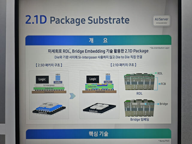
Samsung Electro-Mechanics and LG Innotek are acutely aware of this gap. Samsung has been developing EMIB substrate samples for several years, according to people familiar with the matter, and is now reframing its effort under a 2.1D packaging concept that combines bridge embedding with Reconfigured Distribution Layer techniques. LG Innotek has already begun sample deliveries to SK Hynix and is testing EMIB-T substrates alongside HBM stacks to characterize performance.
Both companies are betting that their existing scale in traditional substrate production — Samsung Electro-Mechanics reported sharply rising utilization rates in the first half of 2026 — gives them a credible entry path. But scaling volume and mastering yield are two different things.
Who Wins If Korea Succeeds
The most important implication of this move is not technical — it is geopolitical and commercial. Advanced substrate supply is currently concentrated in Japan, Taiwan, and Austria. Korea has been largely absent from the high-end segment, focusing instead on memory and display components. Breaking into EMIB-T substrates would give Korea the first foothold in a tier of semiconductor manufacturing that directly serves the AI hardware race.
For Intel, a second source for EMIB-T substrates is a strategic imperative. Over-reliance on Ibiden creates single-point-of-failure risk in a supply chain already strained by capacity constraints and geopolitical tensions. A Korean supplier, while slower to mature, diversifies the base without ceding architectural control — since the substrate must still conform to Intel’s EMIB-T specifications.
For Google and other AI chip designers, more qualified substrate suppliers means stronger negotiating position and potentially lower costs as competition among suppliers intensifies. The AI infrastructure buildout is scaling faster than any single supplier can accommodate.
For Korea, the upside is significant but conditional. The capital required is steep. Ibiden’s 2 trillion won commitment is described as conservative by industry observers; meaningful capacity expansion in advanced substrates runs well beyond that. Samsung Electro-Mechanics and LG Innotek would need to match or exceed that commitment while simultaneously managing competing priorities in their existing businesses.
The Timing Is Tight
Google’s next-generation TPU launch window in late 2027 creates a hard deadline. Any Korean supplier hoping to capture volume from that shipment needs to pass qualification, ramp production, and demonstrate yield stability well before then. That leaves roughly 18 to 24 months — an aggressive timeline for a technology where incumbents have a decade of production data.
The risk is real. A failed qualification cycle or persistent yield issues could strand the investment and leave both companies with advanced substrate capability but no customers. The alternative — staying on the outside of this supply chain — means watching the highest-growth segment of semiconductor manufacturing expand without a Korean participant.
Neither option is comfortable. But the direction of the bet is clear: Korea is choosing to spend heavily now rather than pay a premium later for access to technology it cannot influence.
Whether that calculus pays off depends on how quickly Samsung and LG can close the gap with companies that built theirs one year at a time.