Memory Is Eating GPUs — Samsung and SK Hynix Make Their Bets
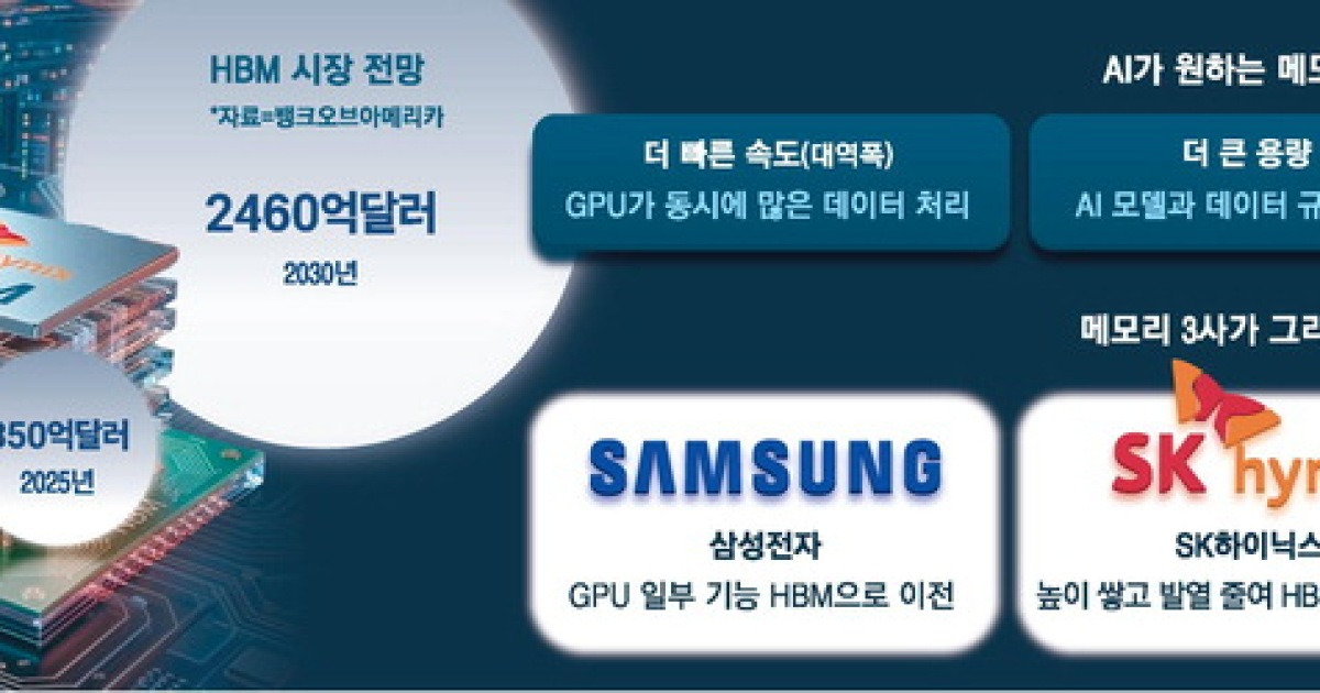
At Hot Chips 2026, Samsung and SK Hynix revealed opposing strategies to break the memory wall: Samsung is turning HBM into a compute element, while SK Hynix is stacking it higher and cooling it smarter. The winner will define who designs the next generation of AI chips.
The memory that computes
For decades, memory was the quiet support act in the AI chip story. GPUs did the math; HBM just held the numbers until the GPU asked for them. At Hot Chips 2026 at Stanford, that arrangement looked ancient.
The memory session — the first time the conference carved out a standalone track for it — was less a technology update than a succession announcement. Samsung and SK Hynix, Korea’s two chip giants, sat side by side and laid out opposite answers to the same problem: the memory wall is eating AI training and inference alive, and the only way through it is to stop treating memory as memory.
Samsung’s play: make HBM think
Samsung’s pitch was the bolder one. Han Sang-wook, a technical leader at the company, described turning the base die at the bottom of every HBM stack from a passive data conduit into an active processing element built on advanced logic fabs. In plain terms: the chip that used to just route data now runs a slice of the GPU’s workload.
The logic is hard to argue with. GPUs are spectacular at math and miserable at waiting. A growing share of their cycle budget disappears managing data movement through HBM rather than doing the actual matrix multiply. If the memory stack can absorb even a fraction of that data-management overhead, the GPU is freer to compute and the system sips less power for the same job.
Samsung laid out a three-stage road map culminating in zHBM — a vertically integrated memory-plus-compute block where the GPU and HBM are bonded as one unit. The company claims zHBM would cut power by roughly 70 percent compared with HBM5. That number is ambitious and not independently verified; it also assumes the logic layer can be fabricated at competitive yields inside Samsung’s own foundry, which remains a variable.
Samsung can make this bet because it owns the full chain: DRAM design and manufacturing, logic design, and its own foundry business. It can draw a architecture on paper and then build it.
SK Hynix’s play: stack higher, cool smarter
SK Hynix took the opposite route. Rather than redesign what HBM is, it is making HBM taller and cooler. Lee Jae-sik, the company’s Americas vice president, highlighted hybrid bonding to stack more than 20 layers of DRAM and i-HBM, a targeted cooling approach that chills the hot spots in a stack instead of re-engineering the whole thing.
It is a packaging-first strategy, and that is no accident. SK Hynix depends on external foundries — primarily TSMC — for its advanced logic, so restructuring the base die as a processor is structurally harder for it. What SK Hynix controls best is the craft of stacking and interconnect. If the winning move is to pack more bandwidth into a smaller footprint with better thermal management, SK Hynix’s instinct is sound.
The rivalry is sharpening because both paths converge on the same outcome: memory stops being a commodity and becomes a co-designed system component. The company that shapes the interface first — between its HBM and a customer’s GPU — gains leverage over the next generation of AI accelerators.
The economics behind the engineering
Jim Handy of Objective Analysis put the financial dimension bluntly. The 2026 memory bottleneck, he said, is not a technology problem but a money problem. Demand for HBM has surged with AI investment, and fab capacity has not kept pace. Price and supply are now the binding constraints, not physics.
That shifts the battlefield. When a component is scarce, the supplier who can offer a differentiated product commands more power. Standard HBM is a race to the bottom on price per gigabit. Custom memory designed together with a chip maker is a race to the top on system performance — and to the bottom on how much margin the memory supplier can extract.
Meta’s appearance at the same conference reinforced the point. Working with AI chip startup D-Matrix, Meta unveiled a 3D DRAM concept that fuses a custom DRAM block directly under its compute chip. The claim: data travel distance drops to a fraction of what HBM requires, cutting data-movement power to about one-sixth of HBM’s level while pushing bandwidth to 100 terabytes per second.
A customer building its own silicon is not a friendly signal for any memory vendor. It tells Samsung, SK Hynix and Micron that dependence on standards alone is no longer a safe business model.
Who wins, who loses
The near-term winner is any AI chip maker that can lock in HBM supply. Capacity constraints mean orders placed today translate into shipments six to twelve months from now; delays cascade through product launches. SK Hynix, already the dominant HBM supplier to NVIDIA, has an incumbent advantage that Samsung must overcome with performance leaps, not just volume.
Samsung gains if its zHBM road map delivers. The 70 percent power claim, if even half-true, would be compelling for cloud operators running margin-thin inference workloads. But Samsung must also prove it can produce logic dies at the bottom of HBM stacks at yields competitive with its foundry customers’ expectations — a tall order when the fab mix is still maturing.
SK Hynix gains if packaging and thermal management become the binding constraints faster than architectural innovation. Stacking 20 layers is hard; keeping them from cooking themselves is harder. i-HBM targets exactly that problem, and thermal limits are becoming real bottlenecks in dense AI racks.
The bigger loser may be the old division of labor itself. Memory was a commodity business with predictable cycles. System co-design is a relationship business with longer sales cycles, deeper customer entanglement and higher switch-cost loyalty. Both Korean companies are converting from vendors into platform partners — which means they also become easier to replace if a chip maker decides to go in-house, as Meta appears to be doing.
What happens next
Three things to watch over the next 18 months.
First, whether Samsung ships a working base-die logic prototype. Announcements are cheap; silicon is expensive. A tape-out with competitive power and yield numbers would force SK Hynix and Micron to respond architecturally, not just dimensionally.
Second, whether NVIDIA or another dominant GPU maker adopts a Samsung-style integrated block or sticks with a modular HBM stack. The anchor customer’s choice sets the industry standard for a decade.
Third, how much capital flows into HBM-specific capacity. Handy’s point about money, not technology, being the bottleneck suggests that expansion decisions this year determine supply dynamics through 2028. Samsung and SK Hynix are both planning large investments; who spends first and fastest may capture the margin window before demand normalizes.
The memory wall is not a metaphor anymore. It is the constraint that will separate the AI systems that scale from the ones that stall. At Hot Chips 2026, Samsung and SK Hynix made clear they intend to be the ones holding the wall up.