Qualcomm Just Turned Samsung and SK Hynix Against HBM's Throne
Qualcomm announced that Samsung and SK Hynix are now actively developing a rival memory architecture alongside HBM — a sign the AI memory monopoly is cracking. The move reshapes the entire supply chain.
The day HBM got a challenger
At the Deutsche Bank Technology Conference on September 26, Qualcomm’s senior vice president Durga Malladi revealed something most English-language desks missed: Samsung and SK Hynix are now actively developing a new memory architecture called HBC — and they’re doing it right alongside their HBM programs.
This is not a polite acknowledgment of competition. It is two of the world’s largest memory manufacturers doubling down on a design that Qualcomm explicitly framed as a replacement for HBM.
The context matters. At Qualcomm’s investor day in June, senior vice president Tony Palkas argued that the GPU-plus-HBM model was hitting a hard ceiling. GPUs and HBM constantly shuttle data back and forth, generating enormous heat and consuming more power than AI model growth can sustain. HBM, Palkas said, had structural limits. The industry needed something else.
HBC is that something else.
What HBC actually is
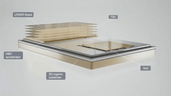
HBC stacks multiple low-power DRAM chips vertically on top of an accelerator chip — what Qualcomm calls an XPU — with the compute die serving as the foundation. Data moves through silicon via through-silicon vias, similar to HBM’s stacking approach, but the architecture shifts computation closer to the memory rather than treating them as separate components passed data between.
Qualcomm’s numbers are aggressive. On the same power budget, HBC delivers six times the bandwidth efficiency and six times the token processing throughput compared to equivalent HBM configurations. Against conventional GPU systems, token throughput under identical power constraints is up to eight times higher. Compared to SRAM — the fast but expensive memory used in some AI accelerators — HBC holds a total cost of ownership advantage.
Malladi confirmed that first-generation HBC products are scheduled for commercial shipping next year, integrated into Qualcomm’s AI250 AI accelerator. A second-generation version, AI300, is planned for 2028 with an enhanced compute die designed to widen the performance gap against next-generation HBM.
The surprise was the partners’ reaction
Here is where the story gets interesting for anyone tracking the AI chip supply chain.
Malladi said Qualcomm initially expected Samsung and SK Hynix to push back hard after the June investor day presentation criticized HBM’s limitations. Instead, both companies came to Qualcomm with active proposals to cooperate on HBC development. They are now pursuing both strategies in parallel — HBM roadmap commitments and HBC engineering — rather than choosing one path.
That signals a fundamental shift in how memory manufacturers view their own products. HBM has been their crown jewel, the high-margin differentiator against Micron and older DRAM lines. To see the two biggest HBM producers willingly invest in an alternative architecture suggests they see HBM’s dominance as conditional, not permanent. The question is whether AI demand will grow large enough to accommodate both architectures, or whether one will displace the other entirely.
Qualcomm’s play: design without manufacturing
Qualcomm is not building HBC alone. The company’s role is deliberately narrow: it designs the compute die that sits beneath the stacked DRAM, provides the TSV integration design, and handles system-level architecture. Samsung and SK Hynix handle the DRAM chip stacking. TSMC will manage packaging and final integration.
This division of labor is strategic. Qualcomm avoids the capital intensity of memory manufacturing while retaining control over the intellectual property that differentiates its accelerators. It also keeps TSMC close — a relationship that gains importance as TSMC’s dominance in advanced packaging faces increasing competition from Samsung’s own I-Cube platform and Intel’s foundry ambitions.
The first product, AI250, ships next year. The second, AI300, lands in 2028 with a more powerful compute die. Qualcomm also indicated that HBC integration into its Dragonfly C1000 data center CPU is technically feasible, though no timeline was given.
Why this matters beyond Qualcomm
HBC is being positioned as a general-purpose technology, not a data-center-only solution. Malladi said Qualcomm is developing form factors suitable for smartphones, tablets, PCs, extended reality headsets, and automotive systems — essentially every category where on-device AI is becoming a competitive requirement.
That timeline is consistent with Qualcomm’s typical product cycle: a device category enters planning and discussion today, and HBC-powered products reach consumers roughly three years later. Meaning the consumer implications of this architecture will not be visible until 2028–2029.
But the supply chain implications are already unfolding. If HBC proves viable at scale, it changes the value proposition of every player in the AI memory ecosystem. HBM manufacturers lose exclusivity over the high-bandwidth memory slot. Accelerator designers gain an alternative that does not require HBM’s pricing premium. Foundries that specialize in advanced packaging — TSMC included — become critical gatekeepers rather than optional suppliers.
The fact that Samsung and SK Hynix are pursuing HBC alongside HBM, rather than replacing it, suggests the near-term outcome is coexistence. But coexistence is fragile. If HBC reaches performance parity at lower power and cost, the economic case for HBM weakens rapidly — especially for clients who cannot justify HBM’s premium for inference workloads that do not demand peak training throughput.
Who wins, who loses
Qualcomm wins by anchoring a new architecture to its own accelerator roadmap while forcing memory manufacturers to compete on its terms. Samsung and SK Hynix win by maintaining relevance in a potential post-HBM landscape and preserving relationships with a major fabless chip designer. TSMC wins as the packaging integrator, though its margin depends on HBC not being absorbed into Samsung’s own packaging capabilities over time.
HBM suppliers other than Samsung and SK Hynix — notably Micron — face the sharpest threat. If HBC becomes a credible alternative, Micron’s HBM pricing power weakens regardless of its technical merits. NVIDIA, which has bet heavily on HBM-dependent GPU designs, also faces long-term risk if the industry shifts toward near-memory computing architectures that do not require HBM at all.
The Chinese chipmakers watching this develop from afar have another variable to consider: HBC’s supply chain, while less concentrated than HBM’s, still depends on TSMC for final packaging. That creates both an opportunity and a constraint.
What happens next
Watch the AI250 shipment timeline closely. Next year’s production volumes will indicate whether Samsung and SK Hynix are investing in HBC out of genuine conviction or simply hedging against Qualcomm’s leverage. Watch whether other accelerator designers — AMD, Intel, or even NVIDIA — adopt HBC or double down on HBM. Watch whether the architecture reaches consumer devices by 2028 as Qualcomm’s timeline suggests, or whether manufacturing complexity slows deployment.
One thing is clear: the assumption that HBM would remain the uncontested king of AI memory is no longer guaranteed. Qualcomm just handed Samsung and SK Hynix a reason to build an alternative — and in doing so, changed the shape of the market they were supposed to protect.