Why High-NA EUV Is the New Battleground for Leading-Edge Chips
Intel and ASML are racing to commercialize High-NA EUV lithography, a technology that could redefine who controls the most powerful chips. Korea's 2028 bet on the same tooling tells a different story about where the next advantage lies.
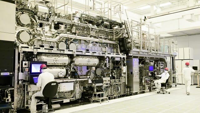
The equipment nobody talks about is about to change everything
Intel and ASML announced accelerated cooperation on High-NA EUV lithography at a conference in Monterey last week. On the surface, it was another industry event. Behind it sits the single most consequential technology decision facing the semiconductor industry right now.
High-NA EUV increases the numerical aperture of extreme ultraviolet lithography from 0.33 to 0.55. The difference sounds small. It is not. A higher NA means finer features can be printed directly, without the multi-patterning steps that currently force fabs to run the same layer two, three, even four times. Fewer passes mean higher yields, lower cost per transistor, and the ability to push nodes below what current EUV equipment can reach.
Intel says it has already processed more than one million wafers through the High-NA EUV system at its Hillsboro facility in Oregon. Some layers of the Core Ultra Series 3 processor — built on the 18A node — are now being manufactured with the new tooling. Intel’s claim is straightforward: performance matches or exceeds conventional EUV layers at 1.8 nanometer-class process.
That claim matters more than the number itself. If true, it means the earliest High-NA EUV production runs are already delivering tangible results. And it means the companies that cannot access this equipment — China’s foundries, in particular — will fall further behind.
The stitching problem nobody is solving easily
Here is what the announcement does not emphasize enough: High-NA EUV cannot expose a large die in a single shot. The exposure area is smaller than previous generations. For chips that are too big to fit inside that window, fabs have to use stitching — breaking the pattern into sections, exposing each separately, and aligning them precisely when reconnecting.
Intel and ASML are pursuing two paths. The near-term path extends 6-inch mask usage with stitching. The long-term path moves toward 6-by-12-inch large masks, which would reduce the number of seams and improve yield. Neither path is trivial. Stitching introduces alignment errors. Large masks require new equipment, new process windows, and new defect inspection methods.
This is why the transition to High-NA EUV will not be instantaneous. It is not simply a matter of buying machines. It is a matter of rebuilding entire process flows.
Korea is betting on the other side of the tool
Samsung has stated it plans to introduce High-NA EUV for memory production in 2028. That timeline is two years behind Intel’s current deployment. But Samsung is not waiting passively. The company is already working with ASML on photomask development and has signaled that High-NA EUV will enter its 1-nanometer process line.
The timing tells a story. Samsung is positioning High-NA EUV specifically for memory — HBM, next-generation DRAM — rather than general-purpose logic. That is a deliberate choice. Memory chips have different layout constraints than CPU or GPU dies. They can tolerate stitching differently. They benefit from finer pitch in ways that may not require the largest possible exposure field.
SK Hynix, Samsung’s rival in memory, is likely following a similar path. Both Korean firms are treating High-NA EUV as a memory acceleration tool, not a general logic play. That leaves logic manufacturing — where AI chips live — to TSMC and, increasingly, to Intel.
Who wins, who loses
The winners from this shift are obvious: ASML, which faces enormous demand for its EXE:5000 systems; Intel Foundry, which gains a differentiated capability it can offer to customers; and Samsung, which secures a head start in memory-focused High-NA EUV deployment.
The losers are less visible but potentially more significant. Chinese semiconductor manufacturers such as SMIC already operate without access to High-NA EUV equipment. The technology gap they face is widening. Advanced chip design tools from companies like Synopsys — which recently reported a 22 percent reduction in AI chip design effort for Samsung’s 2-nanometer process — are also restricted from China. The combined effect is a manufacturing floor that cannot keep pace with the leading edge.
Taiwan faces a different kind of pressure. TSMC dominates advanced logic fabrication, and the US has been pushing to shift that capacity to American soil. High-NA EUV deployment in Oregon gives Intel a potential foothold in that effort. Whether it becomes a structural advantage depends on whether Intel can sustain yield improvements at scale.
What happens next
The next twelve months will reveal whether High-NA EUV can deliver on its promise for logic chips beyond the initial demonstration layers. Intel’s 18A process is the test case. If the tooling proves reliable across multiple layers and through volume production, other foundries will accelerate their own timelines. If defects and alignment issues persist, the industry may delay adoption and look for incremental improvements to current EUV instead.
For Korea, the question is whether the 2028 memory deployment timeline creates a competitive window or a vulnerability. If AI chip demand continues to outstrip supply, memory bottlenecks could slow the entire ecosystem. High-NA EUV could help — but only if Samsung and SK Hynix can move fast enough to meet the demand curve.
The technology is not just about finer transistors. It is about who controls the floor where the next generation of computing gets built. The companies and countries that figure out High-NA EUV first will set the terms for years to come.