Intel's Diamond Rapids: 256 Cores and 1.28GB Cache Redefine Server CPUs
Intel has unveiled Diamond Rapids, a next-generation Xeon server processor packing 256 cores and a staggering 1.28GB of last-level cache. Built on a new 3D tile architecture using Intel 18A-P, it signals a major leap in datacenter computing power.
A Monster Takes Shape
Intel did not announce Diamond Rapids quietly. At the Hot Chips conference on August 25, the company revealed what amounts to its most aggressive datacenter processor to date — a chip with up to 256 cores and an astronomical 1.28GB of last-level cache. The specification alone is worth the headlines. That cache is large enough to hold a significant operating system image in memory. It is also a clear signal that Intel intends to dominate the high-end server segment with raw scale.
Western coverage so far has been sparse. But the details emerging from the presentation tell a coherent story about where Intel is heading with its x86 server strategy, and what it is willing to do to stay competitive against AMD and the growing pressure from ARM-based architectures like Ampere and Amazon Graviton.
How Diamond Rapids Is Built
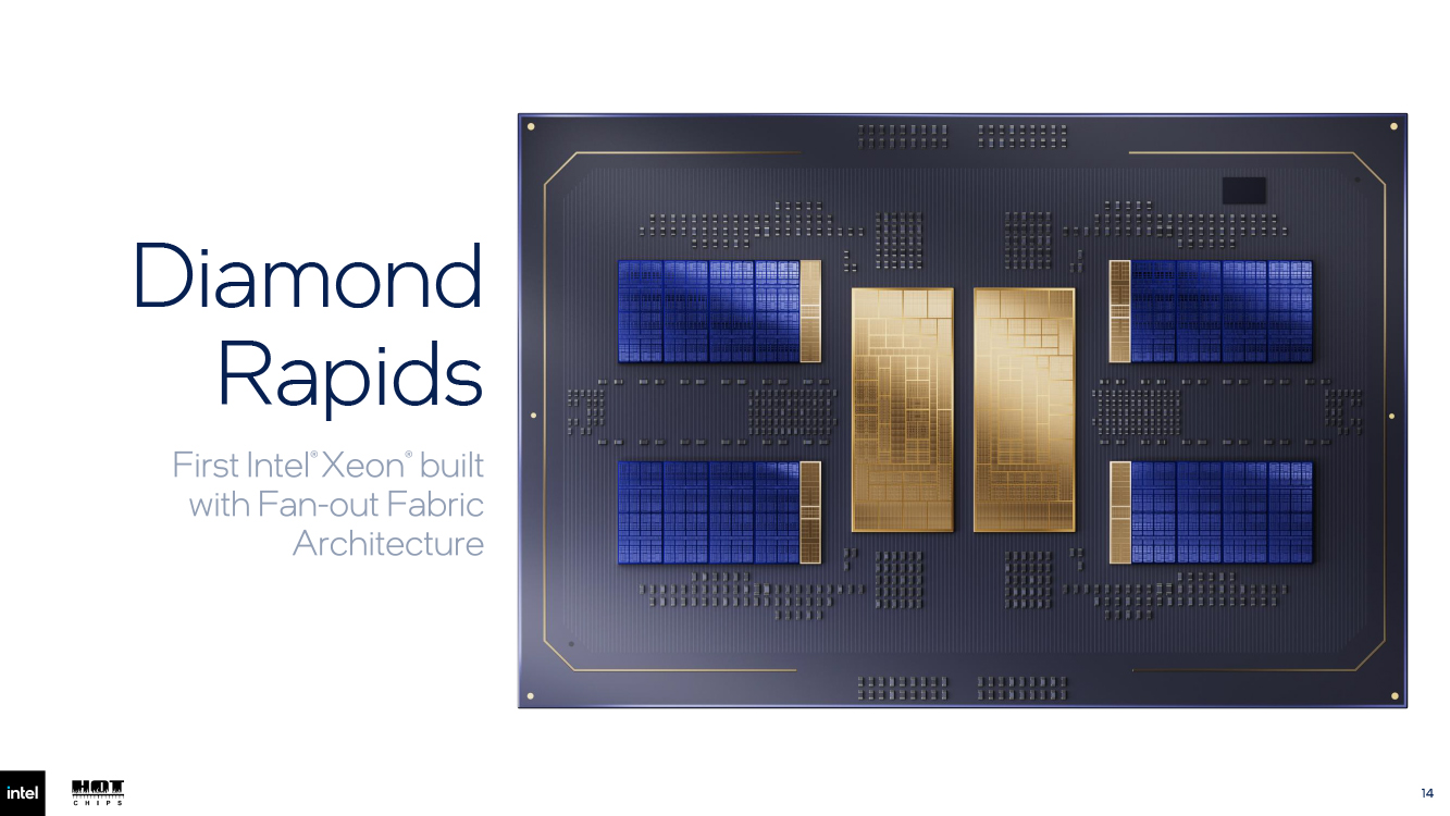
Diamond Rapids abandons the monolithic die approach that defined earlier Xeon generations. Instead, it relies on what Intel calls a Fan-out Fabric architecture — a design that separates the compute logic from the memory and I/O fabric and links them with high-bandwidth interconnects.
The foundation is the Compute Building Block, or CBB. Each CBB houses four core chiplets stacked vertically above a base tile. The vertical connection uses what Intel calls a Hybrid Bonding Interface, built on its Foveros 3D Direct packaging technology. This mirrors the philosophy behind AMD’s 3D V-Cache: shorter vertical paths mean lower latency and less energy when cores talk to their shared cache.
The base tile then connects horizontally to a Fabric Hub tile via a Die-to-Die Interface using UCIe-S at 16G, running over copper traces on the substrate. This horizontal bus carries memory traffic and I/O traffic between the compute blocks and the rest of the system.
The tile-level partitioning matters because each block can now be manufactured on the process node that best fits its function. The core chiplets use Intel 18A-P, a derivative of the 18A process seen in the consumer Panther Lake Core Ultra 3 series. The base tile uses Intel 3-T, and the Fabric Hub uses standard Intel 3. This is the chiplet model working as originally intended — optimizing cost by matching process to purpose.
What 18A-P Actually Means
Intel 18A-P is not a consumer chip process. It is a targeted refinement of 18A for high-performance, low-power logic. Intel claims several improvements over the base 18A node: an additional fifth logic voltage threshold option between ULVT and LVT, a 33 percent reduction in manufacturing performance variance, and specific gains of 18 percent in power reduction, 9 percent in performance, and 20 to 40 percent in thermal resistance improvement.
Power management is divided into four independent DVFS domains — Core, CBB uncore, I/O, and Memory — allowing the chip to throttle or boost individual sections independently. The Core and CBB uncore domains have gained a new idle state that preserves L2 cache while prioritizing turbo clock behavior. These are subtle but important refinements for a chip that could draw significant power under load.
The Core Count and Memory Configuration
Each core chiplet holds up to 16 cores. Four chiplets sit on one base tile, creating a CBB with 64 cores. Four CBBs fit in one package, reaching the 256-core maximum. Memory support scales to 16 channels of DDR5 at up to 8,000MT/s, or MRDIMM at 12,800MT/s, delivering a peak memory bus bandwidth of 1.6TB/s.
That bandwidth figure is not abstract. It positions Diamond Rapids to feed the kind of memory-hungry workloads — large language model inference, real-time analytics, in-memory databases — that have been squeezing traditional server designs dry.
For AI acceleration, the chip supports AMX and AVX-10.2 instruction sets, including FP8, FP16, and BF16 data types. This means CPU-bound AI inference workloads, which have grown increasingly important as model sizes and serving demands shift, can run natively without offloading to discrete accelerators in every case.
Connectivity and Expansion
Diamond Rapids provides 128 lanes of PCIe 6.0, along with CXL 3.0 support and UPI 3 for multi-processor scaling. Eight additional PCIe 4.0 lanes are available for legacy or low-bandwidth peripherals. Security features include TDX and TDX Connect for confidential computing, SGX for enclave execution, and hardware accelerators for QAT, DSA, and IAA.
Perhaps the most practically significant feature for software engineers is the enablement of Intel APX — Advanced Performance Extensions. Announced in 2023 but not yet fully realized in shipping silicon, APX doubles the number of general-purpose registers, introduces three-operand instructions that eliminate redundant data copies, and adds support for conditional instructions and 64-bit absolute branches. The net effect is a measurable reduction in instruction count for certain workloads, achieved without changing application code beyond recompilation.
Who Wins and Who Loses
The immediate winner is any datacenter operator running workloads that scale with core count and benefit from massive on-die cache. Database administrators, cloud providers running large in-memory datasets, and AI inference operators will find Diamond Rapids directly relevant. The 1.28GB cache could meaningfully reduce memory access latency for cache-sensitive applications, which is often the bottleneck in real-world deployments.
AMD’s current leading EPYC processors, while also using chiplet designs, do not yet match this core density or cache capacity in a single socket. That gives Diamond Rapids a performance advantage in the very high end, at least on paper.
Intel’s ARM competitors, including Ampere and Qualcomm, face renewed pressure. The question for them is whether software ecosystems built around ARM can justify the switch when x86 offerings like this continue to close the performance gap while preserving existing code compatibility.
What Happens Next
Diamond Rapids has not shipped. The Hot Chips announcement was a architecture reveal, not a product launch. Actual availability, pricing, and performance numbers will come later. Intel’s claims about 18A-P improvements are factory-spec figures; independent verification will matter.
But the architectural direction is unmistakable. Intel is investing heavily in 3D packaging, process diversity across tiles, and cache hierarchy expansion. The strategy is not to chase clock speed alone but to build a processor that can absorb complexity through scale and smart memory organization. If execution matches the blueprint, Diamond Rapids could redefine expectations for what a single-socket x86 server processor can do.