Korea Invented PLP. Now It May Lose Control of the Standard
Samsung first commercialized panel-level packaging, but with no official size standard, TSMC is quietly consolidating the ecosystem around its own spec. Korea's fragmented supply chain risks becoming a captive supplier.
The First-Mover’s Dilemma
Samsung Electronics holds the distinction. It was the first company in the world to commercialize fan-out panel-level packaging, or FO-PLP — and it already shipped the technology in the Galaxy Watch application processor. That sounds like a commanding lead. But commanding positions in semiconductors don’t survive on first-mover status alone. They survive on ecosystem gravity. And right now, that gravity is pulling toward Taiwan.
The problem is not that Korea cannot make PLP. The problem is that nobody in Korea has convinced anyone else which size PLP actually matters.
Panels Without a Standard
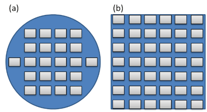
A 300mm silicon wafer is about as standardized as hardware gets in this industry. Every fab, every equipment maker, every material supplier has spent decades optimizing for one circle. PLP broke that pattern. It replaced the wafer with a rectangle — a panel — which eliminates the wasted kerf around the edges and lets manufacturers pack more chips per run. For AI processors that are growing larger every generation, that geometry is a genuine advantage. Thermal performance improves. Unit output climbs.
But unlike the 300mm wafer, PLP panels have no agreed-upon size. According to industry sources cited by Electronic News, there are now more than 30 different panel dimensions in circulation worldwide — 310 by 310 millimeters, 415 by 510, 600 by 600, 700 by 700, and more. Each came from a different conversion line, originally built for substrates or LCD glass, repurposed for packaging without coordination.
The consequence is exactly what you would expect from fragmentation. Equipment makers receive competing size specifications from different packaging firms. They cannot standardize their tooling. Yields drop because every run requires reconfiguration. Development costs multiply because no single size has earned enough volume to justify deep investment.
What makes this worse is that the cost of staying fragmented is compounding. Every additional panel size that enters the market dilutes the return on investment for any single one. Equipment manufacturers who bet on 415 by 510 millimeters today may find themselves with idle capacity tomorrow if the market coalesces elsewhere. Material suppliers face the same trap — developing a resin formulation or copper plating process for one dimension that may never achieve the volume needed to amortize R&D costs. The result is a low-investment equilibrium where no one dares to commit deeply, and no one can prove that their chosen size will win.
Taiwan’s Playbook
TSMC did not arrive at this moment by accident. While Korean suppliers scatter across sizes, TSMC picked one. It selected the 310 by 310 millimeter panel as its pilot-line standard for high-end PLP and pulled its ecosystem along behind it. Equipment makers, material suppliers, and OSAT partners all converged on that dimension because TSMC’s demand made it the only rational bet.
This is not new. TSMC has done this repeatedly. The 300mm wafer era was shaped the same way — TSMC committed volume, and the global supply chain rearranged itself around the fab’s preferences. The difference now is that the playing field is new. PLP is an emerging standard, not a settled one. Whoever anchors the ecosystem at this stage gets to define it.
TSMC’s approach has also been quietly reinforced by its relationships with AI customers. Large fabless companies designing next-generation GPUs and AI accelerators are beginning to specify their packaging requirements around TSMC’s announced PLP roadmap. When a major customer designs for a particular panel format, the entire downstream supply chain follows. This is how standards harden — not through committees or papers, but through the accumulated weight of customer orders, equipment purchases, and qualified material lists.
Korea entered PLP first. Taiwan is defining PLP now.
The Temptation to Follow
Some voices in the Korean industry are openly discussing a strategy of alignment: conform to TSMC’s 310 by 310 millimeter spec, reduce the barrier to entry, and capture market share as a supplier within TSMC’s orbit. It is a pragmatic argument. If no standard exists, adopting the dominant one removes uncertainty and makes Korean equipment and materials immediately usable by the world’s largest customer.
Pragmatic, yes. Dangerous, also yes. Because alignment is not the same as leadership. If Korea cedes the standard-setting role, its equipment and material companies become captive suppliers in a Taiwan-centric supply chain. Samsung’s ability to differentiate through proprietary packaging disappears. The country that invented the technology ends up purchasing its own innovation back at a premium.
There is also a less visible second-order effect. When a supply chain reorients around a foreign anchor, domestic capability degrades over time. Equipment companies that were once pushing the boundaries of PLP manufacturing begin optimizing for TSMC’s requirements instead. Their R&D agendas shift. Their talent pools retrain. Their institutional memory of alternative approaches fades. Even if Korea wanted to reclaim leadership later, the organizational and technical knowledge required to do so would have atrophied.
The high-end PLP market is expected to take off next year as AI chip demand intensifies. This is the window. Once TSMC’s 310-millimeter ecosystem locks in — once equipment manufacturers have built their lines, once material suppliers have qualified their products, once AI customers have designed around that format — the cost of switching grows steep. Korea would not be negotiating from equality. It would be negotiating from dependency.
What Samsung Must Do
Industry experts quoted in the source material agree on the remedy, even if executing it is far harder than stating it. Samsung needs to prove it can mass-produce high-end PLP at stable yields and then use that proof to convene a standard. The company has already been adjusting panel dimensions over several years, weighing warpage against productivity, but it has not yet locked in an internal baseline — much less announced one externally.
The sequence matters. First, Samsung secures large-volume orders from AI big-tech customers using a specific panel size. Second, it publishes that size and a production roadmap. Third, it guarantees long-term volume commitments and joint investment to domestic equipment and material suppliers. Only then does the ecosystem have a reason to consolidate rather than fracture.
There is a third step that deserves more attention. Samsung must create a competitive moat around its standard that makes imitation costly. This could mean locking key intellectual property into processes that are difficult to reverse-engineer, securing exclusive supply agreements with critical material vendors, or establishing a certification regime that rewards compliance with Samsung’s specific manufacturing requirements. Without these defensive measures, a published standard becomes a free guidebook for competitors rather than a platform for leadership.
Without that sequence, the market will consolidate around whoever has the largest customer — and right now, that is TSMC.
Why This Matters Beyond Korea
This is not only a Korean competitiveness story. PLP is likely to become one of the defining packaging architectures for the next generation of AI chips. If the industry fragments across thirty incompatible panel sizes, every company that depends on advanced packaging — Apple, NVIDIA, Amazon, Google — faces higher costs and slower time-to-market. A coordinated standard, whether led by Korea or Taiwan, serves the entire supply chain.
But coordination without a clear anchor point is just another word for hesitation. And hesitation is exactly what TSMC is exploiting.
The broader implication extends to how the global semiconductor industry allocates standards power in emerging technologies. For decades, the United States and Europe set the rules for chips, software, and interfaces — often through open consortia and published specifications. PLP is one of the first post-Moore’s-law domains where that model has not taken hold. Instead, a single fab has moved fast, anchored an ecosystem, and created de facto standards without ever publishing a white paper or convening a working group. If this pattern repeats across other advanced packaging architectures, the industry will find itself adrift in a series of proprietary silos rather than ascending toward a shared technological frontier.
Samsung’s FO-PLP gave Korea the opening. The question is whether it will close it — or let someone else write the rules.