SK Hynix's H-TPU Is a Quiet Play to Redefine the AI Hardware Stack
SK Hynix isn't trying to beat NVIDIA at their own game. With H-TPU, the memory giant is carving out a new role at the intersection of storage and AI inference — one that could quietly rewire how data centers are built.
The bottleneck is no longer the GPU. It’s the SSD.
SK Hynix knows this better than anyone. The company supplies the memory that feeds NVIDIA’s GPUs and Google’s TPUs — the HBM stacks, the LPDDR chips, the NAND that underpins every major AI training run. But while the rest of the industry races to make GPUs faster, SK Hynix has been watching a slower, quieter problem fester inside every AI data center: the SSD controller.
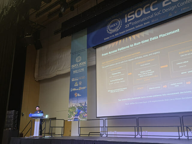
At ISOCC 2026 last week, the memory giant unveiled its answer. Not a bigger GPU. Not a faster CPU. Something entirely different called H-TPU — the Hynix-Transaction Processing Unit.
The pitch is deceptively simple. The problem it solves is structural.
Why SSD controllers are the new bottleneck
Every time a new generation of GPU arrives, its performance roughly doubles. PCIe bandwidth keeps pace. But the control logic inside a typical SSD — the little CPU that decides how to route read and write requests, manage wear leveling, handle error correction — hasn’t kept up. It’s still running on a monolithic, general-purpose CPU architecture that was designed decades ago for a world where storage was slow and simple.
SK Hynix’s Ku In-jae, the company’s vice president of SoC design, put it bluntly. Traditional approaches — just throwing more CPU cores at the problem — lead to extreme power waste and unpredictable pipeline latency. One hundred or so discrete functions that an SSD controller must manage simultaneously simply don’t fit inside a single processor block without serious penalties.
The result is a growing performance wall. AI inference workloads, which are increasingly reading-heavy (some environments show read-to-write ratios approaching 300,000:1), demand that storage controllers respond with deterministic, low-latency precision. General-purpose CPUs are the wrong tool for that job.
What H-TPU actually is
H-TPU is not an AI accelerator. It doesn’t do tensor math. It doesn’t train models or run inference directly. What it does is something perhaps more important for the economics of AI deployment: it controls the data path between storage and compute with extraordinary efficiency.
SK Hynix’s approach was to take the idea of a transaction processing unit — a processor specialized for a narrow class of workloads — and slice it into dozens of tiny clusters. Each H-TPU core uses a lean four-stage pipeline with no superscalar execution and no out-of-order logic. The result is a chip that occupies roughly 1/25th the area and consumes 1/25th the power of a comparable general-purpose CPU core.
The key insight is function-based partitioning. Instead of a single CPU running everything at reduced speed, the controller delegates specific tasks to dedicated processing blocks. Modules involved in write operations stay active; idle modules drop into minimum-power states. The system achieves what SK Hynix calls deterministic, predictable completion times — exactly the property that AI inference workloads need most.
The Hardware Automation layer
There’s a second dimension to H-TPU that matters even more than the silicon itself. SK Hynix described a trajectory toward what it calls Hardware Automation — a layer where repetitive, low-level storage operations (command processing, address lookups, temporary buffer copying) are moved entirely off the processor and into fixed hardware circuits. The CPU and H-TPU then handle only the exceptional cases: errors, policy decisions, and higher-order logic.
This is a fundamental architectural shift. It mirrors what happened in the transition from general-purpose processors to ASICs in the first generation of AI accelerators, but applied to the storage controller — a layer the industry has largely taken for granted.
If SK Hynix executes this vision, the SSD controller stops being a passive pipe and becomes an intelligent, adaptive component of the AI data path. That has implications far beyond storage.
Why HBF changes the calculus
The H-TPU announcement was paired with SK Hynix’s push into HBF — High Bandwidth Flash, a next-generation NAND-based memory product that combines massive capacity with high-bandwidth servicing architecture. This is where the real strategic play becomes visible.
AI inference is overwhelmingly read-dominated. The classic pattern is: load the model weights once, then serve billions of read requests against them. HBF is designed for exactly this workload. When combined with an H-TPU-controlled SoC, the system can prefetch data and manage buffers ahead of time, hiding NAND’s inherent access latency behind the computation pipeline.
SK Hynix’s claim is bold but technically coherent: the controller preserves request context across the entire service path, effectively converting raw NAND flash capacity into usable AI memory resource. In practical terms, this means less reliance on expensive HBM for certain inference workloads and a path to lower total cost of ownership in data centers.
Who wins, who loses
The most obvious winner in this scenario is SK Hynix itself. The company has spent years at the top of the memory chart — DRAM and NAND alike — while the compute story belonged to NVIDIA, AMD, and Google’s custom silicon. H-TPU and HBF represent a move up the stack: from supplying the memory that others’ processors consume, to building the intelligence that orchestrates how that memory flows.
NVIDIA won’t be displaced by an SSD controller chip. But the architecture SK Hynix is describing does challenge the assumption that memory and compute are separate layers that can scale independently. If storage can prefetch, manage buffers, and hide latency intelligently, the pressure on compute-only solutions — and the memory bandwidth they require — loosens slightly. That’s a marginal shift, but in data center economics, marginal shifts compound.
Google, which already designs TPUs and has deep experience in domain-specific controllers, is the closest comparison. But SK Hynix’s advantage is different: scale. The company is the world’s largest memory manufacturer. Its relationship with every major cloud provider and chip designer is already established. H-TPU is not a speculative bet — it’s a vertical integration move backed by real manufacturing volume.
The losers, if there are any, are the companies that benefit most from the current separation of memory and compute layers. SSD controller IP vendors like Phison and Silicon Motion face a direct challenge. So do companies selling the assumption that faster GPUs are the only lever worth pulling.
What happens next
SK Hynix did not announce a shipping date or a commercial customer for H-TPU at ISOCC. The presentation was architectural — a signal, not a product launch. That’s appropriate for a first reveal, but it also means the proof will come in the next 12 to 18 months.
The critical test is whether cloud providers adopt the HBF + H-TPU combination as a standard inference acceleration path. If they do, SK Hynix becomes more than a memory supplier — it becomes a co-designer of the AI hardware stack. If they don’t, H-TPU remains an interesting architecture paper and the status quo holds.
Either way, the direction is clear. The AI hardware race is no longer just about who makes the fastest GPU. It’s about who controls the entire data path — from the GPU’s memory bus all the way down to the NAND flash. SK Hynix just declared that it intends to control the bottom half.