Japan's First 300mm SiC Wafer Could Shift EV Power Supply Chains
Resonac has become the first Japanese firm to publicly exhibit a 300mm SiC substrate, a move that could reassert Japan's position in the race for next-generation power electronics ahead of Chinese and American competitors.
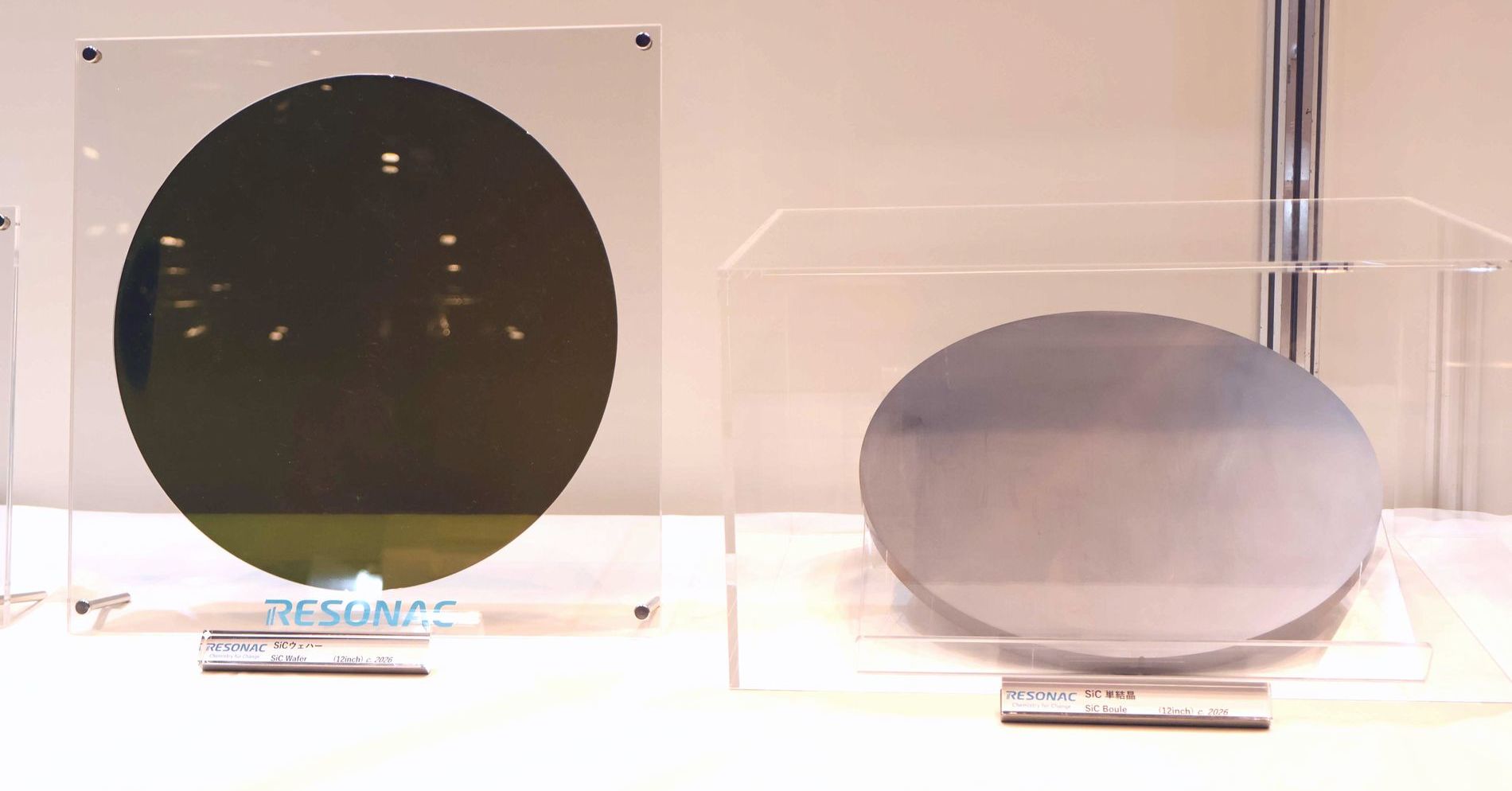
Japan Just Made Its Move in the Global SiC Race
Resonac, the chemical and materials spinoff that inherited much of Hitachi’s semiconductor legacy, did something quietly significant at the International Conference on Silicon Carbide and Related Materials (ICSCRM) 2026 in Yokohama: it became the first Japanese company to publicly display a 300mm SiC single-crystal substrate.
The company announced the development on September 15 and showed the actual ingot and processed wafer to attendees between September 27 and October 2. No one was under any illusion that this was a finished commercial product line — Resonac explicitly stated it has no current plans to develop or sell 300mm epitaxial wafers. But the substrate itself, and the know-how embedded in its manufacture, is real. And its implications stretch well beyond a single manufacturer’s roadmap.
The Thermal Challenge No One Talks About Enough
The reason 300mm SiC substrates are so hard to make has nothing to do with raw ambition. It is a physics problem.
SiC crystals grow at temperatures exceeding 2,000°C. When you scale a boule from 200mm to 300mm in diameter, the thermal gradient between the center and the periphery becomes wildly不均匀 — literally the difference between a usable wafer and a cracked nightmare. Temperature uniformity across that kind of surface area is extraordinarily difficult to maintain during the prolonged crystal-growth cycle that SiC demands.
Resonac said it solved the problem through iterative refinement of furnace conditions and process adjustments. It also upgraded its slicing and polishing capabilities, which matters because SiC is one of the hardest and most brittle materials used in semiconductor manufacturing. Cut it aggressively and you get micro-fractures. Polish it carelessly and you ruin the surface flatness that downstream device fabrication requires.
The company’s own characterization of its competitive edge — “good balance between quality and cost” — sounds like standard corporate modesty. But in SiC substrates, where yield rates can determine whether a fab is profitable or bleeding cash, balance is exactly the metric that separates leaders from laggards.
Why the Timing Is Not Accidental
While Resonac was working through its thermal control challenges, two formidable competitors were making their own 300mm announcements.
China’s SICC — already one of the world’s largest SiC substrate producers by volume — has been pushing aggressively into larger-diameter substrates as part of Beijing’s broader push to control the materials layer of power semiconductor supply chains. America’s Wolfspeed, despite its well-documented financial and operational turbulence, has also publicized 300mm SiC progress, betting that next-generation electric vehicle and grid-scale storage demand will reward the company that first achieves high-yield mass production at that scale.
Resonac’s debut does not overtake either of them. But it does mean Japan — which has been largely absent from the 300mm SiC conversation compared to its dominance in earlier generations of substrate manufacturing — is no longer invisible in this tier. That matters because the next three to five years of EV power electronics buildout will be decided by who can deliver consistent, high-quality 300mm wafers at scale, not just who can announce a breakthrough in a conference hall.
What Resonac Is Really Building — and What It Isn’t
Here is the part English-language readers are likely to miss: Resonac is not treating 300mm as a standalone product line right now. It is treating it as a learning platform.
The company will apply the crystal-growth and substrate-processing insights gained from 300mm development directly to its existing 150mm and 200mm production lines. That means the immediate beneficiary is not a 300mm customer — it is anyone buying Resonac’s current-generation SiC wafers. Expect incremental improvements in defect density, warp control, and yield across the 150mm and 200mm portfolios, even if the 300mm epitaxial roadmap remains on hold.
Resonac also left the door open for sample shipments of the 300mm single-crystal substrate if customers request them. That is a deliberate hedge: it signals technical capability without locking the company into the capital expenditure required for full commercial production before the market clearly demands it.
Who Wins, Who Loses
The winners from this announcement are anyone who buys SiC substrates from Resonac today — their product quality is about to get a quiet upgrade. Automotive Tier 1 suppliers and IDMs designing next-generation EV inverters and on-board chargers should pay attention, because 200mm SiC wafers with improved uniformity can shave costs out of device fabrication even before the industry fully transitions to 300mm.
The losers are less obvious, which is precisely why this matters. Chinese SiC manufacturers, including SICC and several newer entrants funded by state-backed industrial funds, have been betting on volume and price competition to capture market share while Western firms chased 300mm performance. If Resonac can close the quality gap on 200mm and deliver credible 300mm substrates on a controlled timeline, it raises the bar for competition in a segment where China has been gaining ground rapidly.
Wolfspeed, meanwhile, faces its own existential questions. The American company’s 300mm ambitions have been overshadowed by production delays, debt concerns, and the Trump administration’s decision to place Wolfspeed under foreign ownership through a takeover by a consortium led by Google parent Alphabet and other US investors. Resonac’s disciplined, incremental approach — master 300mm crystal growth, improve current lines, offer samples without overcommitting — may look less glamorous than Wolfspeed’s splashy announcements, but it is the kind of strategy that survives financial cycles.
Why This Matters for All Eight Markets
SiC substrates are not a niche concern. They sit at the intersection of three structural shifts: the global transition to electric vehicles, the buildout of grid-scale energy storage, and the ongoing technological competition between the United States and China. Every major economy with an automotive industry or a clean-energy mandate needs a reliable supply of these materials.
Japan’s entry into 300mm SiC substrate production at this stage is a signal that it intends to remain a meaningful participant in the materials layer of power semiconductor supply chains, rather than ceding that ground entirely to Chinese volume producers or American design-focused companies that outsource fabrication. The question is no longer whether Resonac can make a 300mm SiC substrate. It is whether the company can translate that capability into commercial volume fast enough to shape the next wave of EV power electronics sourcing decisions.
The answer to that will determine whether Japan remains a force multiplier in the global semiconductor materials ecosystem — or becomes another footnote in the story of who controlled the substrates that made the electric age possible.